
Last Wednesday afternoon, I had a technical sync with a customer who builds servers. The board was 16 layers, 3.2 mm thick, main signals at 25G, with a few pairs running 56G.
About halfway through, the SI engineer on the other side put the simulation plot on the screen and asked: for these vias that change layers, are you planning to back-drill them?
Our layout colleague said those vias only pass through two layers, so the stub isn’t long — should be fine.
The other side didn’t answer, just zoomed in. One via runs from L2 to L15, but the signal actually only uses L2 and L3; more than two millimeters below are empty. The curve dips into a notch near 12.5 GHz and drops six dB. A bit earlier, you can also see a small step on the TDR.
The room went quiet for a few seconds. For the next two hours the topic basically circled around that one via. After the meeting I sorted out what we discussed and wrote it here to share.
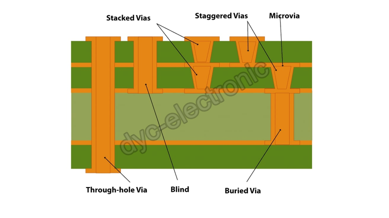
Impedance: That Short Bit of the Via Is Not the 50 Ω You Calculated
A trace‘s impedance is set by width, dielectric thickness, and Dk. A via‘s impedance comes from a different geometry: pad size, antipad clearance, drill size, barrel plating. The two usually don’t agree.
Most through-holes land in 35–45 Ω; a large pad with a small antipad can drop to just over 30 Ω. The reason is simple — between the pad and the plane sits a small parallel-plate capacitor pulling impedance down, while the barrel’s inductance pushes back up, but the via is too short for inductance to win.
A 50 Ω trace with a 40 Ω via in the middle: by the step approximation, (40−50)/(40+50) = −0.11, return loss around 19 dB. On its own that’s not a disaster — but it’s one segment in the whole link, ahead of it sit the connector, the BGA ball, the AC-coupling capacitor, and a few segments stacked up eat the margin.
That day the customer’s 56G pair had its single-ended 50 Ω tuned precisely, yet the differential TDR still showed a step. A differential via’s impedance depends not just on the two signal vias but on the ground vias’ position and count — move them away and the differential loop inductance grows, pulling impedance up.
So via impedance isn’t about “whether to calculate it” — it’s “by what geometry.” Shrink the pad, open the antipad, impedance goes up; open the antipad too much and you cut the return path in the plane. The two pull against each other.
One point often overlooked: the fab’s impedance coupon measures the trace, not the via. A via’s impedance needs a TDR structure or 3D simulation — don’t trust that “50 Ω” line on the report.
Parasitics: Where the Dips and Bumps Come From
A via’s capacitance comes from the parallel-plate between pad and plane; the smaller the antipad, the thicker the board, the higher the Dk, the larger it gets. The inductance comes from the barrel — longer hole, smaller drill, larger inductance.
A standard through-hole runs 0.5–1 pF and ~1 nH. These aren’t fixed — they shift with pad, antipad, thickness, and plating, sometimes by 2×.
At 12.5 GHz, 0.5 pF is only about 25 Ω reactance — the same order as 50 Ω. That “small capacitance” is no longer negligible; it’s yanking the signal toward ground.
Someone at the meeting asked if the pad could be smaller. It can, but a smaller pad tightens the annular-ring and drill-alignment margin — a trade the design and fab work out together.
Together the two parasitics make the via a low-pass section; worse, the impedance drifts with frequency — low frequencies see capacitance, high frequencies see inductance, so the same link sees two different vias.
The Stub: How That Notch at 12.5 GHz Got There
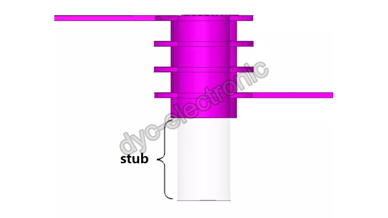
A stub is the unused copper in the via barrel — one end open, the other on the signal. At a quarter wavelength it becomes a short, eating energy and showing as a deep notch in insertion loss; the 3× and 5× harmonics come back too.
With εr≈4, resonance is roughly 37.5 divided by stub length in mm, in GHz. The customer’s via had a 2.8 mm stub — 13.4 GHz; the simulated notch was at 12.5 GHz, close. Real dielectrics aren’t uniform, and pad/antipad loading pulls it down a bit.
Easy to misjudge: the notch is at 13 GHz and Nyquist is only 12.5 GHz — so we’re fine? No. Across that whole span the stub is already eating margin, adding capacitive load, pushing insertion loss up and return loss down, closing the eye — and you haven’t reached resonance yet, so you won’t blame the via.
Back-drilling leaves a 0.1–0.25 mm stub, pushing resonance above several tens of GHz where it’s invisible. Microvias are cleaner — they only connect adjacent layers, no excess barrel through the board. HDI’s value on high-speed boards is more than density.
Return Path: When You Change Layers, the Return Route Breaks
When the signal changes layers, return current must too — from the L2 plane to the L15 plane. With no nearby ground via it detours out to the board-edge decoupling capacitor and back through the power plane. A large loop means more inductance, and radiation and crosstalk rise.
That day we put a ground via within 100 mil of each layer-changing signal via, one each side of a differential pair; where the BGA was too packed, one in the escape direction.
More ground vias isn’t automatically better — position beats count. Return current takes the lowest-impedance path; put the via next to the signal and it uses it, put it far and ten are just decoration.
How to Place Vias Well: 6 Practical Moves
- Change layers less: route on a pair of adjacent layers; every layer change is one more via, one more risk.
- Ground via next to the signal via: especially at layer changes, give the return path a nearby ground via.
- Prefer microvias / back-drilling for high-speed lines: the stub is the high-speed killer; use a short via instead of a long-stub traditional one.
- Control pad and antipad: an oversized pad adds capacitance; set sizes from stackup simulation.
- Don’t pack via arrays too tightly: dense vias crosstalk; leave spacing margin by rate.
- Simulate the critical nets: for GHz signals, verify the via model with SI simulation, stub and return path included.
A Via SI Risk Reference Table
| Via factor | Effect on SI | How to mitigate |
| Low impedance (35–45 Ω) | Reflection, worse return loss | Adjust pad/antipad; verify with TDR |
| Differential via deviation | Differential reflection, mode conversion | Symmetric ground vias; control spacing |
| Parasitic capacitance (~0.5–1 pF) | Local impedance dip, reflection | Shrink pad, optimize antipad |
| Parasitic inductance (~1 nH) | High-frequency bump, reflection | Shorten barrel, parallel ground vias |
| Stub | Quarter-wave resonance, attenuation | Back-drill / microvia |
| Missing return path | Larger loop, EMI/crosstalk | Ground via beside signal via |
| Over-dense vias | Inter-via coupling, crosstalk | Widen spacing, control density |
Frequently Asked Questions
Should via impedance be controlled separately?
Depends on rate. Below 10 Gbps letting the via follow the trace is fine; above 25G treat it as its own structure and simulate it, with a TDR structure on the coupon — the fab’s standard coupon can’t measure the via.
At what frequency should you start worrying about vias?
No red line. When bandwidth (≈0.35 ÷ rise time) passes a few hundred MHz, or rate reaches low-Gbps, stub and parasitics start to matter. Shorter rise time, earlier you manage it.
How long a stub is dangerous?
Tracks your highest frequency. With 37.5/L: to stay clean before 12.5 GHz the stub must be under 3 mm; before 25 GHz, under 1.5 mm. Leave half margin.
How many return ground vias do you need?
One is the minimum, one each side of a differential pair. Some put four around it to suppress loop inductance — not mandatory, but worth it above 25G.
Microvias or back-drilling?
Depends on board and volume. Microvias need HDI — worthwhile at high layer count and density; back-drilling is cheaper on ordinary multilayer boards but leaves a 0.1–0.25 mm residual stub and depth tolerance. Both solve the stub; neither fixes a bad stackup.
Do two-layer boards need to worry about via SI?
Basically no. Slow boards with long rise times have parasitics and stub far below the signal bandwidth — drill freely. Via SI is a high-speed-only headache.
Why These Points Matter
On the schematic a via is a symbol; on the layout it’s a length of conductor. It has an impedance that doesn’t match the trace, carries capacitance and inductance, may drag useless copper that turns on you at some frequency, and cuts the return path when it changes layers.
At low speed these four hide; at high speed they surface together.
I wrote this to ask you: on high-speed boards, do you leave vias to the fab, or model them yourself? How do you weigh back-drilling against reworking the stackup? And do you place ground vias by experience or by rule?
 日本語
 English
 Русский
 Français
 Deutsch
 한국어
 Español
 Português
 العربية
 Türkçe
 Italiano
 Polski
 Dansk