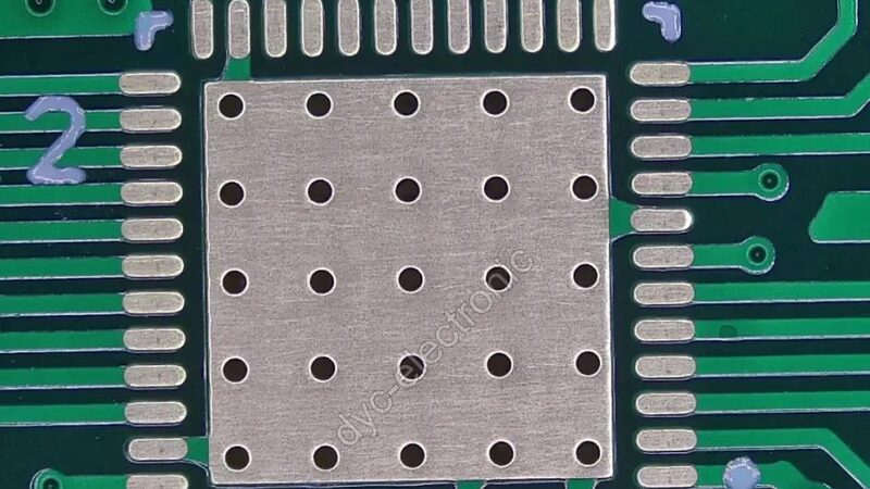
A MOSFET on a 5 W buck converter runs fine on the bench. Bolt it into a sealed enclosure, however, and the same part climbs past 110 °C within minutes. PCB thermal management is what separates a board that survives field use from one that cooks its own solder joints. Actually, heat is not a side effect you fix later. It is a layout decision you make on layer one. Why Your Board Overheats: The Heat Spreading Trap Heat in a PCB follows one unglamorous equation: ΔT = P × R_th. Power dissipated times thermal resistance equals the temperature rise above ambient. Specifically, a 1 oz copper plane on FR-4 […]
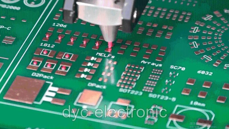
Efficiency and reliability remain top priorities in modern electronics manufacturing. As devices become smaller and more complex, SMT assembly red glue plays a critical role in securing components during production. This epoxy adhesive prevents heavy or double-sided parts from shifting during reflow soldering. Consequently, it bridges the gap between intricate design requirements and manufacturing stability. Understanding this process helps procurement teams balance quality retention with production costs effectively. Understanding the Red Glue Process in PCB Manufacturing Red glue is typically a red-colored epoxy resin used as a temporary bonding agent for Surface-Mounted Devices (SMDs). Its primary function is maintaining component alignment throughout the assembly cycle. Furthermore, the distinctive red color serves a […]
Hand soldering remains a fundamental skill in electronics manufacturing, bridging the gap between schematic design and functional circuitry. This manual process ensures both electrical connectivity and mechanical integrity within electronic assemblies. Whether for prototyping or repair, mastering this technique directly impacts product reliability. Consequently, engineers must understand the core principles of hand soldering to produce high-quality printed circuit board assemblies. Understanding Soldering Fundamentals Soldering joins metal components using a filler material known as solder. This process creates stable electrical contacts while maintaining structural strength. Standard alloys typically consist of tin-lead mixtures, though environmental regulations now drive lead-free adoption. The molten filler acts similarly to adhesive, securing components effectively upon cooling. Therefore, selecting […]
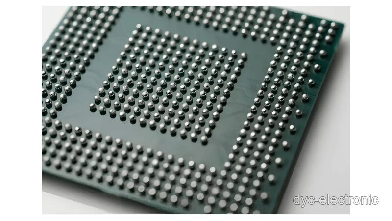
Ball Grid Array (BGA) technology serves as the backbone for modern high-density electronics. Engineers rely on BGA soldering to connect advanced microprocessors and chipsets where traditional leaded packages fail. However, hidden solder joints beneath the component body introduce significant assembly complexity. Consequently, manufacturing teams must adopt precise methodologies to ensure interconnect reliability. This guide details the technical requirements for successful Ball Grid Array integration, from land pattern design to advanced rework protocols. Understanding BGA Packaging Technology A BGA package features an array of solder balls directly contacting the PCB surface. This architecture enables several critical performance characteristics that define modern electronic design. High-Density Interconnections: Manufacturers can package integrated circuits containing over one thousand […]
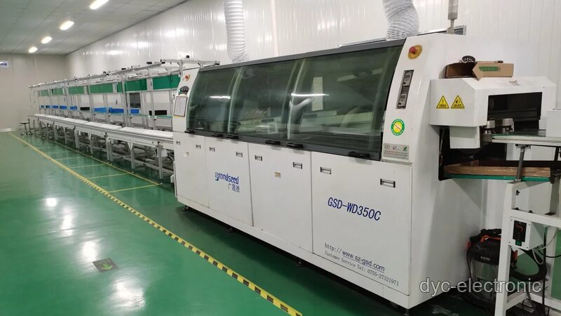
Precision defines modern electronics manufacturing. Consequently, achieving reliable through-hole technology (THT) connections requires specialized tooling beyond basic soldering equipment. The wave soldering fixture design serves as the critical interface between the printed circuit board (PCB) and the molten solder wave. This component, often called a solder pallet, directly influences defect rates and production efficiency. Engineers must understand its function to optimize mixed-technology assembly processes effectively. Importance of Wave Soldering Fixtures in PCB Assembly These fixtures hold PCBs securely while selectively exposing specific areas to the solder wave. Such controlled exposure proves essential for boards combining surface-mount devices (SMDs) with THT components. Without proper shielding, delicate parts risk damage from unwanted solder contact […]
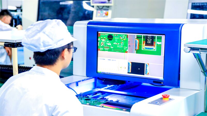
Modern electronic devices demand smaller sizes, faster speeds, and greater functionality. Consequently, printed circuit board complexity has increased dramatically. Dense layouts with fine-pitch packages and thousands of solder joints make manual inspection inefficient and unreliable. Therefore, manufacturers rely on Automated Optical Inspection to guarantee production quality. This technology serves as a critical checkpoint in both fabrication and assembly processes. What Is Automated Optical Inspection? Automated Optical Inspection is a machine-based visual inspection method. High-resolution cameras, controlled lighting, and image processing software scan PCBs to detect defects automatically. The system captures board images and compares them against reference data like CAD files or golden boards. Any deviation signals potential manufacturing issues. This technology applies […]
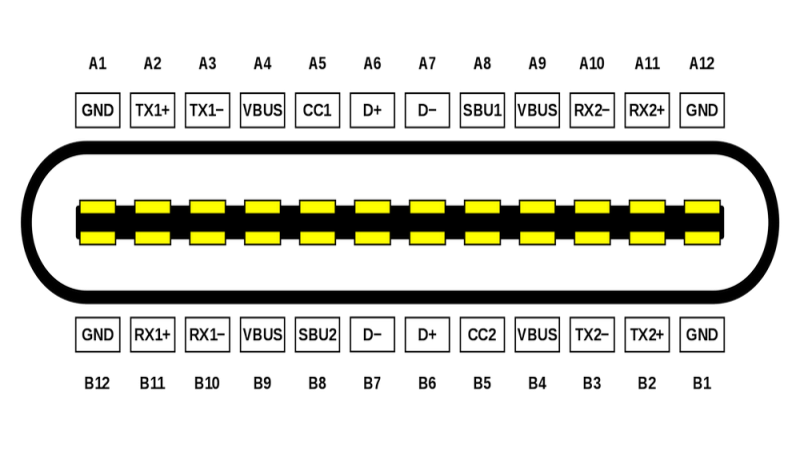
Hardware engineers frequently encounter a critical pitfall in Type-C CC pin configuration: confusing legacy USB-A protocols with native Type-C behavior. Many designers mistakenly treat D+/D- as the core charging channel. Consequently, circuits may show correct 5V polarity yet fail to charge, trigger device recognition errors, operate only on one insertion side, or exhibit current limiting—especially with Apple devices. In nearly all cases, the root cause is incorrect CC1/CC2 termination. Therefore, this guide clarifies standard 5V Type-C CC pin configuration so you can implement reliable charging circuits immediately. Core Principle: CC Pins Are the Sole Charging Channel In any Type-C CC pin configuration, all charging identification, current negotiation, plug orientation detection, and USB Power Delivery […]
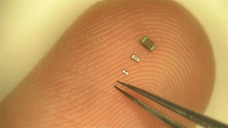
Miniaturization drives innovation across the modern electronics frontier. This trend challenges engineering teams to fundamentally rethink printed circuit board (PCB) manufacturing processes. Among the most complex technologies in this shift is 01005 component assembly. These miniature passive devices measure just 0.4 mm x 0.2 mm, making them the smallest standard surface-mount components currently in mass production. Despite their size constraints, 01005 packages play a pivotal role in designing highly compact devices like smartwatches, IoT sensors, and next-generation smartphones. However, handling and assembling these components introduces significant complexity. This guide explores the specific technical challenges of the assembly process and provides validated solutions for achieving consistent production yields. The Fundamental Nature of […]


 日本語
日本語  English
  Русский
  Français
  Deutsch
  한국어
한국어  Español
  Português
  العربية
  Türkçe
  Italiano
  Polski
  Dansk
Dansk