
AOI vs. X-Ray Inspection: Which Defects Does Each Catch?
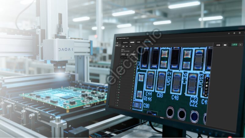
A BGA sits on a medical control board with 400 balls hidden under the body. The AOI vs X-ray inspection question stops being academic the moment a line operator waves the board past the optical camera and it passes — while a 22% void sits inside ball 137, invisible to any lens. We have watched that exact escape reach a customer only once, and it cost a recall. This guide explains, defect by defect, what each method actually sees so you can spec the right coverage before it matters. Engineer’s Note: Treat AOI as proof the board looks right, not that it is right. A clean optical pass says nothing […]
IC Local Ground Plane: EMC Routing Rules & Via Tips
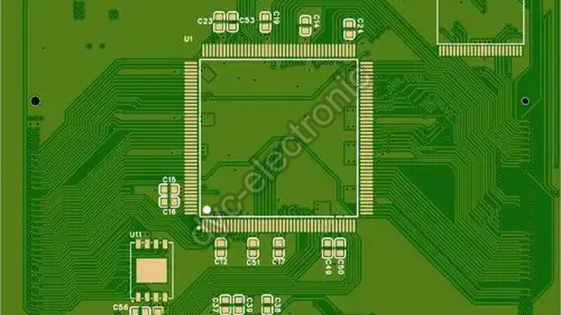
Preserving a solid IC local ground plane beneath high-speed processors is one of the most effective ways to suppress EMI at the source. A 0.5 mm pitch BGA sits on your top layer, and a critical clock trace needs to reach a connector on the opposite side. Do you route directly underneath the package body to save space, or do you maintain an unbroken copper zone? This decision defines whether your board passes EMC testing or becomes a radiating antenna. In our builds, we have seen boards fail CISPR 32 Class B limits specifically because designers routed sensitive signals beneath noisy chips. Actually, the fix was not adding more ferrite beads. It […]
BGA Soldering: Precision Assembly Guide
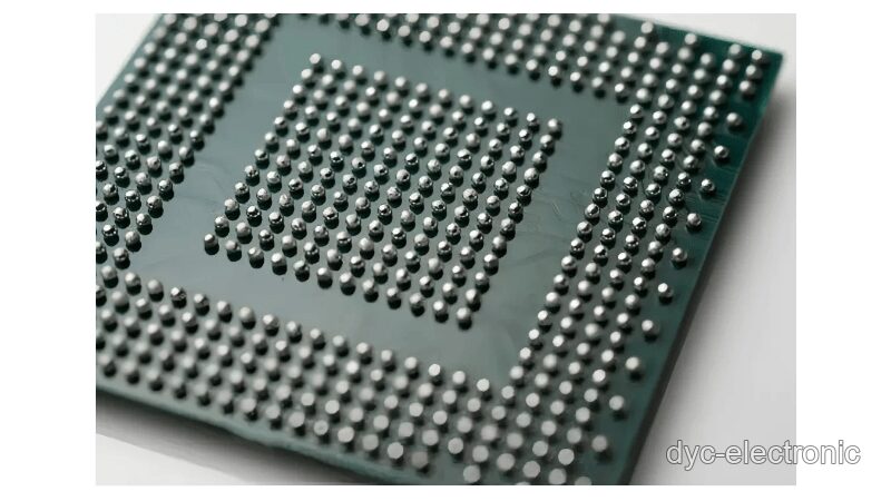
Ball Grid Array (BGA) technology serves as the backbone for modern high-density electronics. Engineers rely on BGA soldering to connect advanced microprocessors and chipsets where traditional leaded packages fail. However, hidden solder joints beneath the component body introduce significant assembly complexity. Consequently, manufacturing teams must adopt precise methodologies to ensure interconnect reliability. This guide details the technical requirements for successful Ball Grid Array integration, from land pattern design to advanced rework protocols. Understanding BGA Packaging Technology A BGA package features an array of solder balls directly contacting the PCB surface. This architecture enables several critical performance characteristics that define modern electronic design. High-Density Interconnections: Manufacturers can package integrated circuits containing over one thousand […]
 日本語
 English
 Русский
 Français
 Deutsch
 한국어
 Español
 Português
 العربية
 Türkçe
 Italiano
 Polski
 Dansk