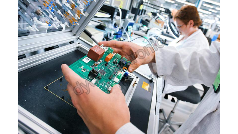
A PCBA box build takes a finished circuit board and turns it into a product you can ship. Short answer: a box build — also called systems integration — mounts the PCBA in an enclosure, adds wiring, power, displays, and firmware, then runs a full functional test so the unit leaves the line ready to […]
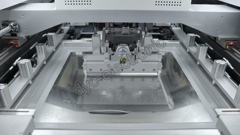
A board passes design review. The paste prints, and a 0.4 mm QFP bridges on three pins. The QFN center pad traps flux gas and voids at 35 percent. None of this shows up in the schematic. It starts at the steel sheet that lays down the solder. SMT stencil design is the discipline that […]
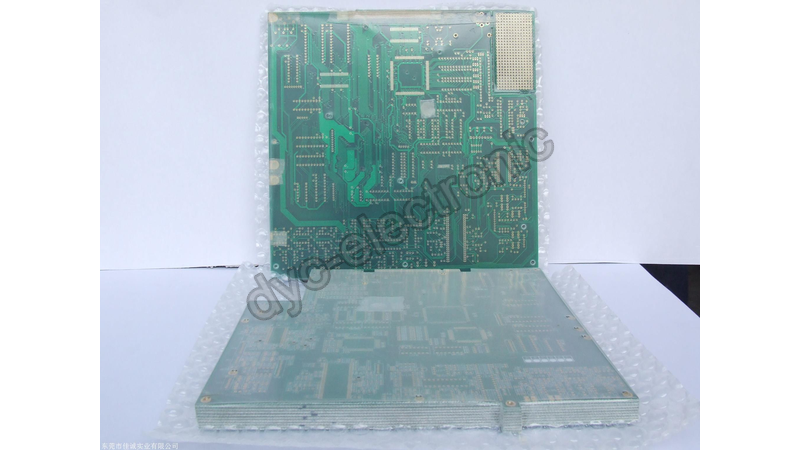
A carton of bare boards lands on a customer’s receiving dock in July. Still, the box looks fine. Inside, one panel has a cracked corner. The pads on a second panel have dulled past their solderability window. And the bag that should have shielded the assembly turns out to be pink poly with no metal […]
A stack of bare boards arrived flat, passed incoming checks, and then bowed after the first lead-free reflow. The BGA coplanarity failed, the placement head scraped a panel, and the line stopped for two hours. PCB bow and twist is the measurement that catches this before it happens: for any board carrying surface-mount parts, IPC-A-600 […]
A customer once sent a drawing marked only “IPC standard, high quality.” Their assembler built to Class 2, the industry default, and the first field returns came from a ventilator program that should have been Class 3 from day one. IPC-A-610 Class 3 is the high-reliability workmanship standard: it demands 100% inspection, complete solder wetting, […]
A procurement lead forwarded a quote that looked 30% below the field. Two weeks later the invoice arrived with a stencil charge, an expedite fee, and a component overage they had never seen. An accurate PCBA quote starts long before the price — it starts with the files you send. Send four things upfront and […]
A buyer emailed at 4 p.m.: the microcontroller on their bill of materials just jumped to a 45-week lead time, and their launch date sits 14 weeks out. PCBA component shortages turn a stable build plan into a fire drill overnight. We have lived this more times than we care to count. In practice, the […]
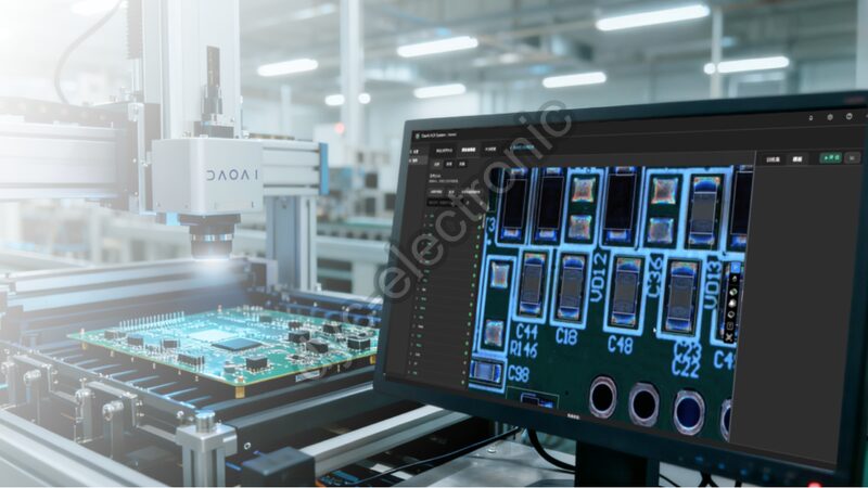
A BGA sits on a medical control board with 400 balls hidden under the body. The AOI vs X-ray inspection question stops being academic the moment a line operator waves the board past the optical camera and it passes — while a 22% void sits inside ball 137, invisible to any lens. We have watched […]



 한국어
한국어  English
  Русский
  Français
  Deutsch
  日本語
日本語  Español
  Português
  العربية
  Türkçe
  Italiano
  Polski
  Dansk
Dansk