
A 0.65mm pitch BGA sits on your layout. You need to escape 800 pins, but through-holes eat every routing channel they touch. Do you jump straight to PCB via types like microvias, or can a smarter stackup save the budget? We review over 200 via specifications weekly, and roughly 40% of boards specified with blind or buried vias could achieve identical routing with through-holes alone. Conversely, defaulting to through-holes when advanced structures are genuinely needed forces extra layers that cost more than the via upgrade itself. This guide gives you the real production cost multipliers, lead time impacts, and decision thresholds from our factory floor—updated as of 2026-09—to help you choose correctly without over-engineering.
Quick Answer: PCB Via Types at a Glance
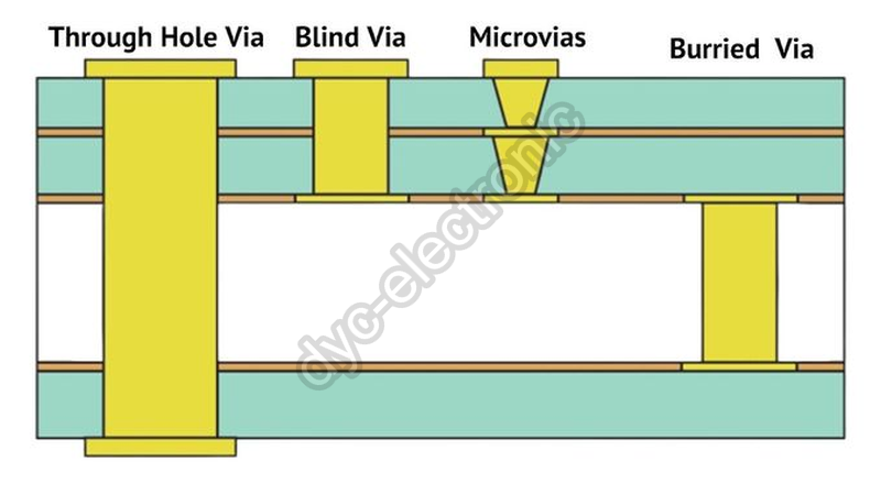
Through-hole vias remain the lowest-cost default for most 2–8 layer boards operating below 10 GHz. Blind vias add 25–35% to board cost plus 3–5 days lead time; they pay off only when BGA fanout demands partial-depth connections on 6+ layer designs.
Buried vias increase cost by 40–60% and add 5–7 days, reserved for 10+ layer boards with extreme inner-layer density.
Microvias (HDI) multiply base cost 2–3× for 1+N+1 builds and become necessary once BGA pitch drops below 0.65 mm.
Backdrilling adds merely 5–10% and eliminates via stubs for signals above 10 Gbps, often proving more economical than switching to blind vias purely for signal integrity. In practice, careful stackup planning lets many designs avoid advanced PCB via types entirely, saving 20–50% on fabrication.
The Via Selection Problem Most Engineers Get Wrong
Selecting PCB via types should be straightforward engineering, yet it consistently drives unnecessary cost in multilayer fabrication. A pattern emerges across customer designs ranging from simple 4-layer industrial controllers to complex 20-layer HDI networking platforms: approximately 40% of boards specified with blind or buried vias could route identically using only through-holes with a more thoughtful stackup arrangement.
The opposite problem also exists. Engineers who default to through-holes on designs that genuinely need advanced structures end up adding layers to compensate for routing congestion. Those extra layers often cost more than the via upgrade would have. Actually, the key is matching the via type to actual design requirements rather than copying a competitor’s reference design blindly.
This guide provides specific cost data, lead time impacts, and decision thresholds. Every number cited comes from our production environment processing boards daily—not theoretical calculations or outdated industry averages. If you want a second opinion before committing, upload your Gerber files for a free DFM review and our engineers will verify whether your current approach is already optimal.
Understanding Via Anatomy: Barrel, Pad, Anti-Pad, and Stub
Before comparing PCB via types, understand what all vias share structurally. Every plated via consists of three functional elements regardless of its span through the stackup.
The barrel is the copper-plated cylinder running through the drilled hole. Barrel plating thickness directly determines current-carrying capacity and thermal cycling reliability. IPC-6012 Class 2 requires minimum 20 µm average barrel plating; Class 3 increases this to 25 µm (IPC-6012). In our production, we target 25 µm minimum for all via types because the marginal plating cost is negligible while reliability improvement under thermal stress is measurable.
The pad (or land) is the copper ring where the barrel meets a trace or plane. Pad diameter minus hole diameter yields the annular ring, which must stay above minimum values for reliable connection. Standard annular ring minimums range from 3.5 mil (89 µm) for outer layers to 3 mil (76 µm) for inner layers under IPC Class 2.
The anti-pad is the clearance hole in copper planes where the via passes through unconnected layers. Its diameter must prevent shorts (typically 8–10 mil larger than drill diameter) yet avoid excessive return-path discontinuity. Finally, the stub is the unused barrel portion extending beyond the last connected layer. On through-hole vias, this stub acts as an unterminated transmission line creating resonant reflections. A 40 mil stub resonates near 18 GHz, but broadband reflections degrade signal edges well below that frequency.
Through-Hole Vias: The Default That Handles Most Designs
Through-hole vias pass completely through the board, connecting all layers. They are mechanically drilled after lamination and electroplated in a single shared process step, which is why they add zero incremental cost beyond standard drilling and plating. For most projects, through-holes remain the correct starting point among PCB via types.
Carbide drill bits range from 0.2 mm (8 mil) minimum up to 6.35 mm for mounting holes. Standard via drills fall between 0.25 mm and 0.35 mm (10–14 mil), producing finished holes of 0.2–0.3 mm after plating. These dimensions accommodate standard design rules while leaving adequate annular ring at typical 0.5–0.6 mm pad sizes.
Aspect ratio—board thickness divided by drill diameter—is the primary manufacturing constraint. At 8:1, plating uniformity begins degrading because chemistry exchange at the barrel center cannot keep pace with the entrance. Most fabricators quote up to 10:1 with standard chemistry; some achieve 12:1 with high-throw processes, but reliability drops measurably above 10:1. For a standard 1.6 mm board, the minimum reliable drill diameter is therefore 0.2 mm (8:1). On 2.4 mm boards, it increases to 0.3 mm.
From our production data, through-holes work well when four conditions hold: ≤8 layers (see our 8-layer PCB stackup design guide for configurations), BGA pitch ≥0.8 mm, signal frequencies <10 GHz without stringent stub requirements, and adequate channel width between via pads. Meeting all four means through-holes serve the design at the lowest possible cost.
Engineer’s Note: Not sure if through-holes suffice? Upload your Gerber files for a free DFM review. Our engineers will analyze your via structures and recommend whether advanced PCB via types would reduce layer count or improve signal integrity—or confirm your current approach is already optimal.
Blind Vias: Partial-Depth Connections for Dense BGA Fanout
Blind vias connect an outer layer to one or more inner layers without penetrating the full board thickness. Visible from one surface only, they free routing space on unreachable layers—valuable when dense package escape routing competes for inner-layer channels. Among PCB via types, blind vias strike a middle ground between cost and density.
Fabrication depends on drill method. Laser-drilled blind vias (depths up to 1–2 layers) use UV or CO₂ lasers to ablate dielectric, followed by electroless and electrolytic plating. Mechanically drilled versions use controlled-depth spindles requiring careful calibration. Sequential lamination offers a third path: inner cores are drilled and plated as through-holes first, then additional layers are laminated on top, converting them into blind structures.
Cost impact is substantial. On a standard 8-layer board, blind vias increase fabrication cost 25–35% over through-hole-only equivalents. This premium reflects sequential lamination presses, extra drilling, additional AOI inspections, and reduced panel yield from tighter registration. At prototype quantities (5–10 pcs), the absolute increase might be $5–8/board; at 500+ pieces, it narrows to $3–5 as setup amortizes. Lead time extends 3–5 working days because sequential lamination cannot parallelize with outer-layer processing.
The practical trigger is BGA fanout. When pitch reaches 0.8 mm or finer on 6+ layer boards, inner ball rows often cannot escape using through-holes alone. However, not every BGA needs blind vias. If pitch is ≥1.0 mm, pin count <400, or sufficient layers exist for through-hole routing channels, blind vias add cost without benefit. This is the most common over-engineering scenario we encounter.
Buried Vias: Inner-Layer-Only Connections for Maximum Density
Buried vias connect inner layers exclusively, never reaching either outer surface. After final lamination they are invisible externally, detectable only through electrical test or cross-section. Their value lies in freeing both outer surfaces for maximum component placement and routing density. Of all PCB via types, buried vias carry the highest fabrication burden.
Manufacturing requires drilling and plating inner cores before final lamination. Individual cores are imaged, etched, inspected, drilled, and plated separately, then stacked with prepreg. Former through-holes in inner cores become buried vias once outer layers encapsulate them.
This process adds 40–60% to fabrication pricing over through-hole-only designs. Combined with blind vias (common in complex HDI), total premium can exceed 80%. Cost drivers include separate drilling/plating/inspection cycles per core, registration maintenance during lamination, and higher yield loss from core-to-core misalignment. Lead time extends 5–7 working days; complex blind-plus-buried builds reach 15–20 days versus 5–7 for through-hole-only equivalents.
From a DFM perspective, the dominant failure mode is registration error between buried via holes and adjacent-layer pads. Thermal expansion during lamination shifts layers 1–2 mil, reducing effective annular ring. Specify minimum 4 mil annular ring (not standard 3 mil) on buried via pads to accommodate this uncertainty. Honestly, buried vias are the most frequently over-specified type we see. In ~60% of designs received with buried via specs, elimination is possible by adding 1–2 layers (often cheaper) or restructuring the stackup. We always check this during DFM review before proceeding.
Microvias and HDI: When Standard Drilling Cannot Solve the Problem
Microvias represent fundamentally different manufacturing technology. Defined by IPC-T-50 and IPC-2226 as ≤150 µm diameter, ≤1:1 aspect ratio, and ≤0.25 mm depth, they are exclusively laser-drilled (IPC-2226). Spanning one dielectric layer only, microvias connect adjacent pairs like L1→L2. Among PCB via types, they enable the finest interconnect densities achievable today.
UV lasers produce smaller, cylindrical holes suitable for diameters <75 µm; CO₂ lasers are faster for 75–150 µm. After drilling, desmear removes carbonized resin, followed by electroless seeding and electrolytic plating. Unlike mechanical blind vias (min 0.2 mm, multi-layer span), microvias fit where drills cannot operate and disrupt surrounding routing far less.
HDI boards use microvias as fundamental building blocks. IPC-2226 classifies builds by microvia layers per side: 1+N+1 adds one buildup layer per side; 2+N+2 adds two. Each level compounds cost and lead time. For detailed breakdowns, see our HDI PCB manufacturing capabilities page. A 1+N+1 build typically costs 2–3× an equivalent non-HDI board; 2+N+2 runs 3–5×. An 8-layer reference board at $15–20/unit (100 pcs, through-hole) becomes $35–50 with 1+N+1 and $55–80 with 2+N+2. Lead time extends 7–10 days for 1+N+1; complex structures take 20–25 days.
Stacked Versus Staggered Microvias
When connections span multiple layer pairs, microvias combine vertically. Stacked microvias align directly atop each other, consuming minimum footprint—essential for fine-pitch BGA fanout where lateral offset blocks escape routing. However, interfaces concentrate thermo-mechanical stress during temperature cycling. IPC-2226 recommends limiting stacks to 2–3 levels. Our IST data shows 2-level stacks achieve 500+ cycles at ΔT=150 °C (meeting IPC-6012 Class 3); 3-level stacks show 10% failing at 300–400 cycles.
Staggered microvias offset each level laterally ≥150 µm, distributing stress and eliminating direct copper-to-copper interfaces. Our IST testing shows 700+ cycles at same excursion—~40% improvement over stacked. The trade-off is space: each offset consumes 150–200 µm routing room, totaling 400–500 µm for three-level transitions. For harsh thermal environments (automotive −40 to +125 °C, industrial, defense), staggered is strongly preferred. For consumer electronics with moderate thermal demands and severe space constraints, stacked is acceptable within IPC limits.
Via-in-Pad: Routing Directly Through Component Connections
Via-in-pad (VIP) places a via inside an SMT pad rather than beside it. This becomes necessary when BGA pitch drops below 0.8 mm because no physical space remains for dog-bone fanout. Among PCB via types, VIP demands the strictest fabrication discipline.
The non-negotiable requirement: vias must be filled and planarized before assembly. Open or partially filled vias wick molten solder away during reflow, starving joints and causing opens or voids. We’ve seen first-pass yield drop below 60% when designs specified VIP without explicit fill notes. Standard solution is VIPPO (Via-In-Pad Plated Over): non-conductive epoxy fill, planarized flat, then copper-plated to create a smooth solderable surface. Conductive fill (copper paste or electroplated copper) costs more but eliminates epoxy’s thermal resistance.
Fill cost adds ~$0.50–1.50/board at 500+ pcs depending on via count and material. This stacks on top of whatever via type cost applies. Use VIP when BGA pitch ≤0.8 mm, thermal pads under QFN/QFP need direct ground-plane connections, or routing density prohibits dog-bone fanout. Skip it when pad pitch allows standard escape—the added cost and yield risk aren’t justified.
Procurement Tip: Complex via structures need DFM verification before fabrication. Upload your design files and our engineering team will verify manufacturability, suggest optimizations, and provide accurate pricing within 24 hours. Submit Design for DFM Review
Backdrilling: Signal Integrity Fix Cheaper Than Blind Vias
Backdrilling mechanically removes unused through-hole barrel portions beyond the last connected signal layer. Result: stub-free performance comparable to blind vias at a fraction of the cost. For high-speed designs evaluating PCB via types, backdrilling deserves consideration before jumping to blind vias.
Physics is straightforward. A via stub creates a resonant notch in frequency response. A 40 mil (1 mm) stub resonates ~18 GHz in FR-4, but insertion loss degradation starts well below resonance. At 10 Gbps (frequency content to 12.5 GHz at fifth harmonic), even 60 mil stubs cause measurable eye closure. At 25 Gbps, stubs >10 mil become problematic.
Backdrilling uses an oversized bit (2–4 mil larger than original hole) to remove stub copper, leaving controlled residual length. Standard tolerance is ±4 mil (100 µm); for 56+ Gbps PAM4, ±2 mil is achievable at higher cost. Cost adds only 5–10% versus 25–35% for blind vias. If motivation is stub elimination rather than routing density, backdrilling achieves the same electrical result at ~⅓ the premium. Lead time impact is minimal: 1–2 days versus 3–5 for blind vias.
Real Production Cost Comparison Table
The following data comes from our quoting system for a reference 8-layer FR-4 board (100×100 mm, 1.6 mm, 1 oz Cu, ENIG, 100-unit qty, 2026-09 baseline $16–20/unit):
One insight many miss: upgrading via type sometimes enables layer-count reduction, yielding net savings. A 12-layer through-hole board switching to 10-layer with blind vias may actually cost less because two fewer copper/prepreg/lamination cycles offset the blind via premium. We find this opportunity on ~15% of justified advanced-via designs.
Decision Framework: Choosing Without Over-Engineering
Rather than abstract guidelines, here are specific thresholds from analyzing thousands of designs. Start with through-holes as default; add complexity only when these conditions exist and stackup restructuring cannot resolve them:
- BGA ≥1.0 mm pitch, <400 pins, ≤8 layers: Through-holes almost always suffice. Escape routing works via dog-bone fanout with adequate inner channels.
- BGA 0.8 mm, 400–800 pins, 8–12 layers: Blind vias justified for inner-row escape. First two rows typically escape with through-holes; rows 3+ need layer transitions blocking fewer channels.
- BGA ≤0.65 mm pitch or >800 pins space-constrained: Microvias (HDI) necessary. No stackup optimization substitutes for laser-drilled footprint when pad spacing <250 µm.
- Signals >10 Gbps, adequate through-hole density: Evaluate backdrilling before blind vias. If simulation shows unacceptable stub resonance, add backdrilling at 5–10% rather than restructuring fabrication at 25–35%.
- ≥10 layers, extreme inner density, surfaces inaccessible: Buried vias become sole option. Verify first whether adding 1–2 standard layers resolves congestion cheaper.
- Thermal pads under QFN/QFP/power packages: Via-in-pad with thermal vias provides lowest thermal resistance. Specify epoxy fill for signal vias; consider copper fill only where heat dissipation is critical.
Cost Note: Get accurate pricing for your specific design. Upload Gerber files and receive a detailed quote breaking down costs by via type, with optimization recommendations that may reduce fabrication expense without compromising performance. Get Detailed Via Quote
DFM Rules by Via Type: What Fabricators Need Right
Each PCB via type introduces specific DFM requirements beyond general rules. Violations don’t always trigger Gerber rejection—sometimes boards simply fail in field after thermal cycling or develop assembly yield problems.
For through-holes, critical parameters are aspect ratio (<10:1 standard, <8:1 Class 3), minimum annular ring (3.5 mil outer, 3 mil inner post-tolerance), and via-to-via spacing accommodating anti-pads. Most common rejection reason: insufficient annular ring at high-aspect-ratio holes where drill tolerances consume available land.
For blind vias, add controlled-depth drill tolerance (±2 mil mechanical, ±0.5 mil laser). Specify target layer clearly—ambiguous depth callouts rank top-five for fabrication queries delaying orders 1–2 days. For buried vias, use 4 mil minimum annular ring to accommodate lamination shift. Consider that thin-core high-aspect-ratio drilling presents different plating challenges than full-thickness through-holes.
For microvias, treat IPC-2226’s 1:1 aspect ratio as maximum, not target. Design to 0.75:1 for better bottom plating coverage. Capture pad ≥100 µm larger than laser hole; target pad ≥75 µm larger. For via-in-pad, specify fill material, cap method, and planarity (typically ±0.5 mil). Missing any specification forces default assumptions that may not match assembly needs.
Common Over-Engineering Scenarios We See Weekly
Specific patterns recur frequently enough to document as cautionary examples:
First, blind vias on 6-layer boards with 0.8 mm pitch BGAs having <300 pins. Outer two rows escape via dog-bone through-holes; remaining inner signals route internally without partial-depth vias. Adding blind vias here adds 25–35% cost with zero routing benefit. Solution: verify escape feasibility on standard stackup first.
Second, buried vias where 1–2 additional layers solve congestion cheaper. A 10-layer buried-via board costs 40–60% above baseline. A 12-layer through-hole-only board costs ~30–40% more than 10-layer baseline—adding simple copper/prepreg without process complexity change. The 12-layer through-hole board is often cheaper AND faster.
Third, HDI microvia builds when only 1–2 fine-pitch BGAs exist amid standard components. Often, fine-pitch areas route with 0.2 mm mechanical blind vias instead, dropping cost multiplier from 2–3× to 1.25–1.35×. On a $20 baseline, that saves $15–33/unit.
Fourth, copper fill specified for all BGA-area vias when only thermal pads need conductivity. Signal vias need only epoxy fill. Separating specs saves $0.30–0.80/board.
Via Reliability: What Thermal Cycling Data Shows
Reliability under thermal stress is the ultimate quality test. Our lab performs IST and thermal cycling per IPC-TM-650 on every new via configuration.
Through-holes with proper plating (≥25 µm barrel) consistently achieve 1000+ cycles at ΔT=150 °C before resistance increase indicates failure. Failure occurs at barrel-to-dielectric transition points. Aspect ratios >8:1 reduce cycle count 20–30% due to cumulative expansion mismatch. Blind vias behave similarly but add base-separation risk where barrel meets landing pad—proper desmear and bottom plating mitigate this.
Single-level microvias show excellent reliability when copper-filled (>1000 cycles). Short length minimizes expansion mismatch. Stacked microvias are the concern point per earlier discussion. Practical takeaway: specify plating thickness explicitly. Minimum 20 µm average / 18 µm minimum (Class 2) suffices for commercial. For automotive/medical/aerospace, specify 25 µm minimum (Class 3) and request IST coupon testing with production lot.
What to Include in Your Fabrication Package
Documentation clarity directly affects quote accuracy, query turnaround, and first-article success. Missing via specs are the #1 cause of fabrication queries, each adding 1–2 days processing.
Specify at minimum: blind via span and drill method preference; buried via connected layers and fill requirements; HDI structure (1+N+1 etc.), stacked/staggered choice, and copper fill needs; via-in-pad fill material, planarization, and specific via subset. Include a drill table distinguishing via types by size and code. Many CAD tools output separate drill files per type—use this feature. If combined, add clear notes identifying which holes map to which PCB via types and layers.
Ready to optimize? Whether reviewing simple through-hole designs or quoting complex HDI builds, our team provides detailed DFM feedback with every quote. Upload Design Files for fabrication-ready recommendations within 24 hours.
Frequently Asked Questions
How much do blind vias add to PCB cost compared to other PCB via types?
Blind vias typically add 25–35% to base fabrication cost versus through-hole-only equivalents. This covers sequential lamination, additional drilling, and extra inspection. On an 8-layer board costing $15–20/piece at 100 units with through-holes, blind vias bring unit cost to ~$19–27. Premium narrows at higher volumes as setup amortizes. Among PCB via types, blind vias sit mid-range in cost—above backdrilling but below buried vias and HDI.
When should I use microvias instead of blind vias for PCB via types selection?
Choose microvias when BGA pitch ≤0.65 mm or pin count >800 in space-constrained designs where mechanical blind vias (min 0.2 mm) physically cannot fit between pads. For 0.8 mm pitch BGAs with moderate pin counts, mechanical blind vias often suffice at 1.25–1.35× cost versus 2–3× for HDI. Microvias become mandatory only when pad-to-pad spacing <250 µm leaves no room for mechanical drill lands.
Is backdrilling cheaper than blind vias among PCB via types for signal integrity?
Yes, in most cases. Backdrilling adds ~5–10% versus 25–35% for blind vias. If primary motivation is stub elimination on high-speed signals rather than routing density, backdrilling achieves identical SI improvement at ~⅓ the premium. Crossover occurs when you need blind vias for BOTH routing density AND signal integrity simultaneously—typically >8 layers with multiple high-speed differential pairs.
What is the maximum aspect ratio for different PCB via types?
Standard through-holes: reliably 8:1, upper limit 10:1 with qualification. Mechanical blind vias: practical limit 1:1 to 0.75:1. Laser microvias: IPC allows 1:1 max depth 0.25 mm, but most fabricators target 0.75:1 for reliable plating. Pushing beyond these limits increases void, crack, and thermal cycling failure risks across all PCB via types.
Do buried vias increase lead time significantly versus other PCB via types?
Yes. Buried vias add 5–7 working days because inner cores require complete drill/plate/inspect cycles before final lamination. Combined with blind vias, total lead time reaches 15–20 days for complex HDI versus 5–7 days for through-hole-only equivalents. This is the longest lead time impact among common PCB via types.
 한국어
한국어  English
  Русский
  Français
  Deutsch
  日本語
日本語  Español
  Português
  العربية
  Türkçe
  Italiano
  Polski
  Dansk
Dansk