
A purchasing manager once sent us a request for “500 PCBs” with a BOM attached, expecting fully functional units. We had to clarify that they actually needed PCB vs PCBA distinction understood before production started. This confusion happens more often than you’d think in electronics procurement. A Printed Circuit Board (PCB) is just the bare foundation, while a Printed Circuit Board Assembly (PCBA) is the finished, functional product with all components mounted. Mixing these terms up can lead to wrong quotes, delayed shipments, and failed prototypes.
Let’s break down exactly what separates a bare board from a complete assembly, so your next RFQ hits the mark.
What Is a PCB? The Bare Foundation
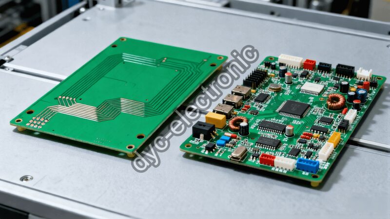
Think of a PCB as the skeleton of your electronic device. It provides mechanical support and electrical connections but contains zero active or passive components. Engineers typically refer to this stage as a “bare board” or “blank PCB.” Without assembly, it cannot perform any function on its own.
These boards are usually made from fiberglass-reinforced epoxy laminates like FR-4. The copper traces etched into the substrate define the circuit paths. Actually, the quality of this bare board directly determines the reliability of the final printed circuit board assembly. If the base material has poor thermal performance or inconsistent dielectric constants, even perfect soldering won’t save the product.
Three Common Types of Bare Boards
Single-layer PCBs have only one conductive layer and suit simple consumer gadgets. They are the most cost-effective option when space isn’t critical. Double-layer PCBs feature copper on both top and bottom surfaces, connected via plated through-holes. Most industrial controllers use this configuration for better routing density.
Multi-layer PCBs stack three or more conductive layers with insulating prepreg between them. High-speed communication devices and medical equipment rely on these complex structures. However, adding layers exponentially increases fabrication complexity and cost. That said, choosing the right layer count early prevents expensive redesigns later.
Engineer’s Note: Always verify the IPC-4101 laminate specification with your fabricator before ordering. Material substitutions without approval cause impedance mismatches in high-frequency designs.
What Does PCBA Mean? Bringing Circuits to Life
PCBA stands for Printed Circuit Board Assembly. This term describes the complete process of mounting electronic components onto a bare PCB to create a working unit. While a PCB is passive, a PCB assembly is active and ready for system integration. The transition from bare board to functional assembly involves precise placement, soldering, and rigorous validation.
Two primary technologies dominate modern assembly lines. Your choice depends on component size, production volume, and reliability requirements. In practice, many projects combine both methods on the same board to leverage their respective strengths.
Surface-Mount Technology (SMT) Process
SMT assembly places components directly onto surface pads without drilling holes. This method enables higher component density and smaller form factors. Our SMT lines typically follow four critical steps:
- Solder Paste Printing: Stencil applies paste to designated pads
- Component Placement: Pick-and-place machines position parts at high speed
- Reflow Soldering: Controlled heat profile melts solder joints simultaneously
- Automated Optical Inspection (AOI): Cameras verify placement accuracy post-reflow
This technology suits mass production of compact consumer and IoT devices. However, SMT joints are mechanically weaker than through-hole connections. Watch the reflow temperature curve closely; exceeding peak temps damages moisture-sensitive components per IPC/J-STD-020 standards.
Through-Hole Technology (THT) for Durability
Through-hole assembly inserts component leads into drilled holes before wave or hand soldering. This creates stronger mechanical bonds ideal for connectors, transformers, and high-stress environments. Military and automotive applications still prefer THT for its vibration resistance.
The workflow includes drilling, lead insertion, soldering, and inspection. Although slower than SMT, THT remains essential for mixed-technology boards. Here’s the catch: each additional hole adds drilling time and reduces routing space on inner layers. Balance durability needs against manufacturability during design.
For detailed process parameters, explore our SMT Assembly Process guide covering nozzle selection and paste viscosity control.
Testing Protocols: Bare Board vs Assembled Unit
Testing strategies diverge sharply between stages. Bare PCBs undergo electrical continuity checks using Flying Probe or Pinned Fixture testers. These verify trace connectivity and detect shorts or opens before components are added. Relatively simple and fast, this step catches fabrication defects early.
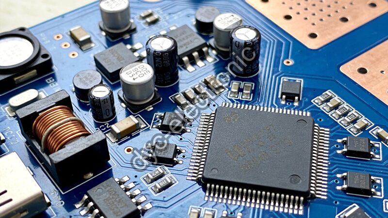
Conversely, PCBA testing validates full functionality under simulated operating conditions. Methods include AOI for solder joint quality, In-Circuit Test (ICT) for individual component values, and Functional Test (FCT) for end-to-end performance. Smoke testing identifies catastrophic failures safely, while regression testing ensures firmware updates don’t break existing features. All tests must align with IPC-A-610 acceptability criteria to guarantee field reliability.
Procurement Tip: Request test coverage reports and first-article inspection data with every shipment. Visual pass/fail stamps aren’t enough for mission-critical assemblies.
Real Cost Drivers in PCB Assembly
Many buyers assume component price dominates total cost. Actually, labor, tooling, and turnaround time often outweigh raw material expenses. Understanding these variables helps optimize budgets without sacrificing quality.
Key factors influencing PCBA manufacturing cost include:
- Bare board complexity and layer count
- Component package sizes and pitch (0402 costs more than 0805)
- Mix of SMT versus through-hole processes
- Order quantity and panel utilization efficiency
- Required testing level and documentation
- Packaging specifications (anti-static, compartmentalized trays)
- Expedited turnaround premiums
Smaller batches carry higher NRE (Non-Recurring Engineering) charges per unit. Conversely, large volumes amortize setup costs effectively. Always ask suppliers to break down NRE separately from unit pricing for transparent comparisons.
Material Selection Impacts Performance and Price
Substrate choice affects signal integrity, thermal management, and long-term reliability. FR-4 remains the industry workhorse due to balanced mechanical strength and cost. For high-speed digital or RF circuits, low-loss materials like Rogers or Teflon reduce signal attenuation despite higher expense. Metal-core PCBs (aluminum or copper base) excel in LED lighting and power electronics where heat dissipation is critical.
In assembly, material compatibility matters equally. Mismatched CTE (Coefficient of Thermal Expansion) between components and substrate causes solder joint fatigue over thermal cycles. Verify that selected laminates meet UL 94 V-0 flammability ratings for safety compliance. Refer to the UL PCB Materials Guide for certified material databases.
When specifying materials for your PCB vs PCBA project, always cross-reference datasheets with actual supplier capabilities. Generic “FR-4” labels hide vast performance differences between manufacturers.
Quick Reference: PCB vs PCBA Comparison Table
Use this table as a sourcing checklist to avoid terminology mix-ups:
Remember: quoting a PCB when you need PCBA results in receiving unusable blanks. Always specify “assembled” or reference part numbers tied to complete builds.
Frequently Asked Questions About PCB vs PCBA
What is the main difference between PCB and PCBA?
A PCB is an unpopulated bare board providing electrical pathways, while a PCBA includes all mounted components and is fully functional. You cannot use a PCB without completing the assembly process.
A PCB is an unpopulated bare board providing electrical pathways, while a PCBA includes all mounted components and is fully functional. You cannot use a PCB without completing the assembly process.
Can I order PCB and PCBA from different suppliers?
Technically yes, but we strongly advise against it. Handoffs introduce risk of damage, contamination, and accountability gaps. Single-source PCB assembly providers manage yield holistically and resolve issues faster.
Technically yes, but we strongly advise against it. Handoffs introduce risk of damage, contamination, and accountability gaps. Single-source PCB assembly providers manage yield holistically and resolve issues faster.
Why does PCBA cost significantly more than bare PCB?
Assembly adds labor-intensive placement, multiple soldering cycles, extensive testing, and component procurement overhead. Even with cheap boards, populated printed circuit board assembly costs reflect true value-added processing.
Assembly adds labor-intensive placement, multiple soldering cycles, extensive testing, and component procurement overhead. Even with cheap boards, populated printed circuit board assembly costs reflect true value-added processing.
How do I know if my quote covers PCB or PCBA?
Check line items carefully. Quotes listing only “board fab” or “bare PCB” exclude assembly. Valid PCBA quotes itemize components, stencils, placement fees, and testing. Ask for clarification if uncertain.
Check line items carefully. Quotes listing only “board fab” or “bare PCB” exclude assembly. Valid PCBA quotes itemize components, stencils, placement fees, and testing. Ask for clarification if uncertain.
Final Thoughts for Smart Sourcing
Understanding the PCB vs PCBA distinction isn’t academic—it directly impacts your budget, timeline, and product success. Bare boards are commodities; assemblies are engineered solutions requiring deep process expertise. Whether you’re prototyping or scaling production, clear communication prevents costly misunderstandings.
 한국어
한국어  English
  Русский
  Français
  Deutsch
  日本語
日本語  Español
  Português
  العربية
  Türkçe
  Italiano
  Polski
  Dansk
Dansk