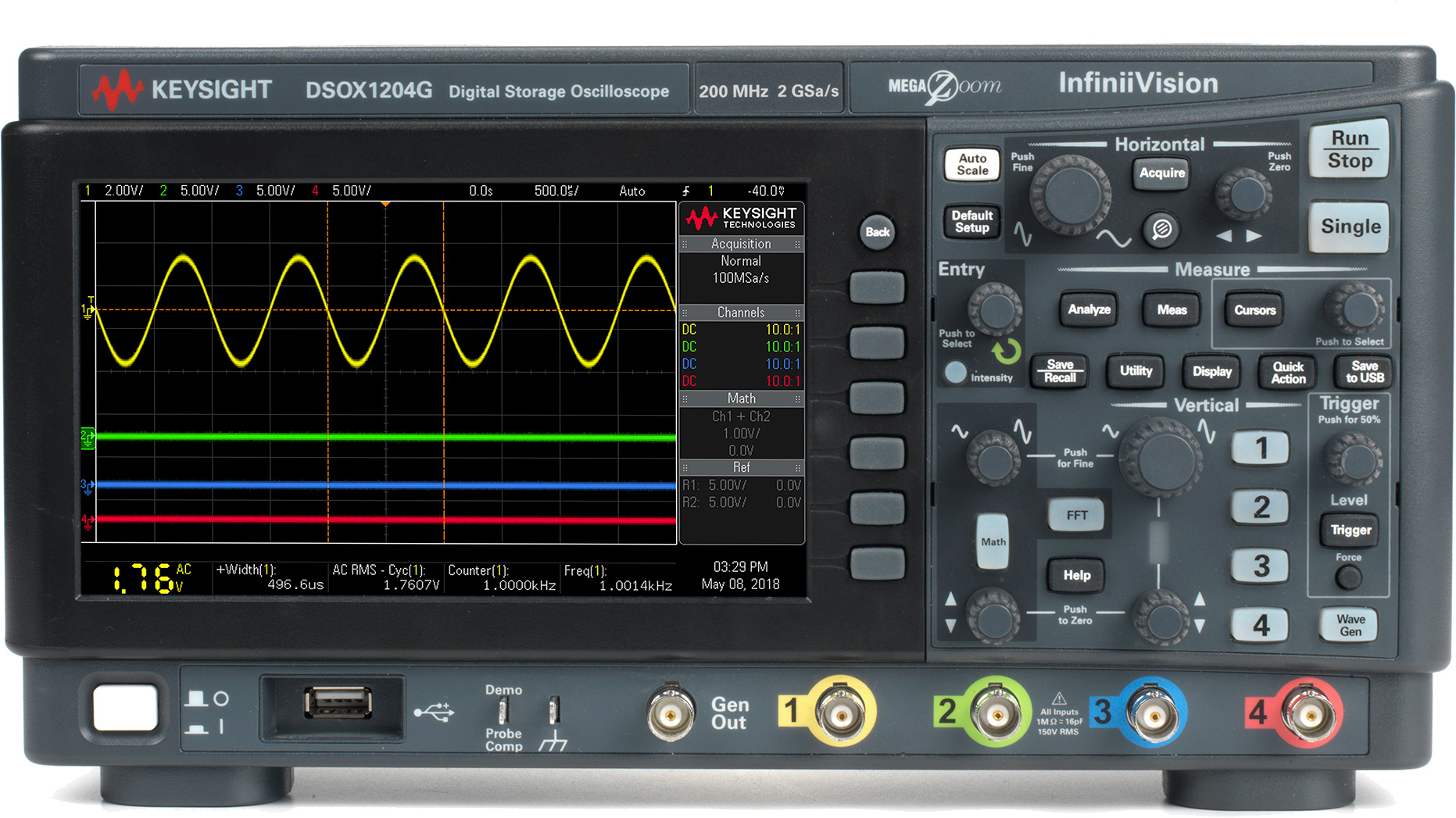
For electronic R&D engineers, an oscilloscope serves as the primary window into circuit behavior. We rely on this instrument to inspect transient electrical signals and validate design performance. However, this “window” can sometimes present a distorted view. In many cases, the displayed waveform does not reflect actual operating conditions. To minimize oscilloscope waveform measurement errors, engineers must master underlying principles rather than relying solely on automated functions. Understanding these mechanisms ensures you capture authentic signal representations consistently. Auto-Set Limitations Causing Oscilloscope Waveform Measurement Errors Nearly all modern oscilloscopes feature an “Auto-Set” button. This function automatically adjusts vertical sensitivity (V/div) and horizontal timebase based on input signals. While convenient for initial visualization, […]
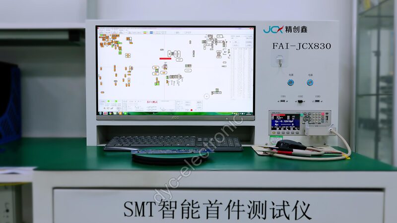
A single misaligned 0402 capacitor on the first board off the line can silently kill an entire production run. We have seen it happen: the reel was swapped during setup, nobody caught the polarity mark shift, and 500 units went through reflow before anyone noticed. That is exactly why first article inspection SMT exists as a mandatory checkpoint. It is not just paperwork; it is the only reliable gate between a correct setup and a costly batch failure. In our builds, we treat this step as non-negotiable, because catching one bad board now saves scrapping five hundred later. Why First Article Inspection SMT Matters on the Line Actually, FAI serves as your […]
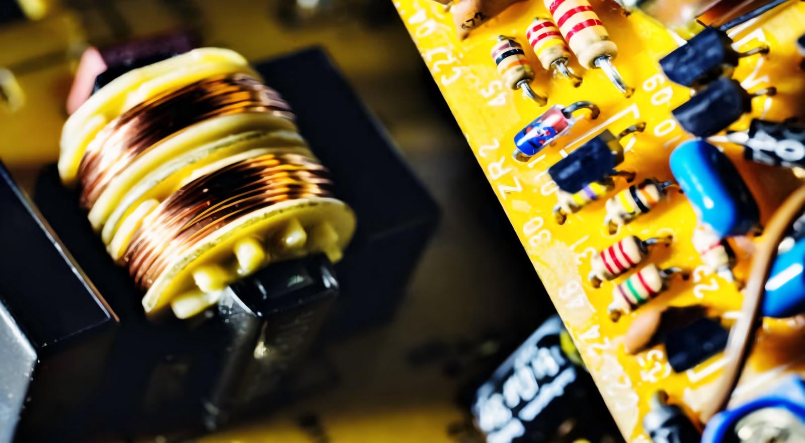
In modern electronic design, printed circuit boards serve as the foundation for everything from consumer gadgets to heavy industrial machinery. Protecting these assemblies from overcurrent events is critical for product safety, reliability, and operational longevity. The PCB fuse acts as the primary defense against excessive current that can cause trace burnout, component destruction, short circuits, or even fire hazards. Selecting the correct protection device distinguishes a robust product from a costly field failure. This guide covers essential technical parameters, selection criteria, and integration practices engineers need to specify the right unit for any application. Whether designing smartphone motherboards, automotive control modules, or industrial power supplies, understanding protection component selection ensures optimal performance […]
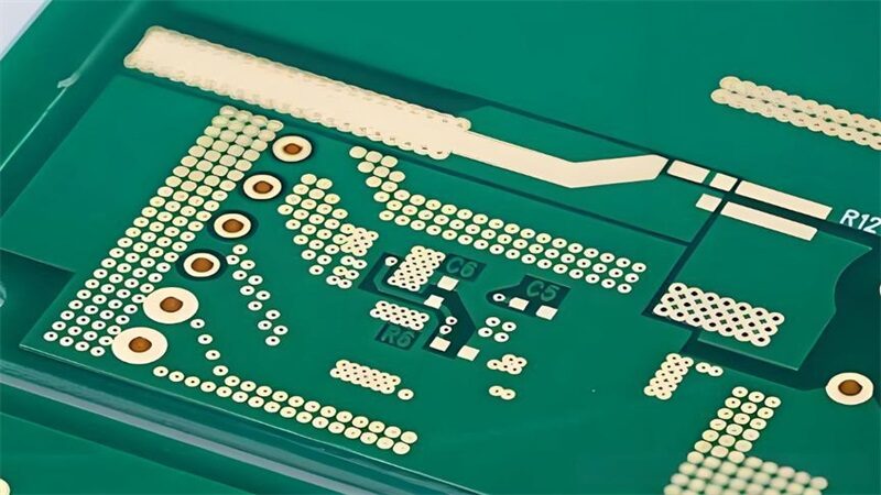
An unpopulated substrate equipped with copper traces, vias, pads, and dielectric layers serves as the fundamental carrier for nearly all electronic equipment. From consumer gadgets to high-performance aerospace systems, medical instruments, and industrial control devices, the bare PCB quality control process determines the final product’s success. Fabrication involves high-precision procedures like lamination, drilling, plating, imaging, etching, solder mask coating, and surface finishing. Each step introduces risks of defects such as broken traces, hidden shorts, uneven plating, or interlayer delamination. If defective boards reach assembly, they cause signal disorders, hardware failures, and safety hazards. Therefore, comprehensive testing is crucial to ensure performance, yield rates, and long-term reliability. Full-Process Bare PCB Quality Control Workflow […]
Reducing PCB assembly cost remains a primary objective for electronics manufacturers facing tight margins. However, aggressive cutting often introduces reliability risks, while pursuing speed without budget controls wastes resources. Sustainable competitiveness requires balancing expense reduction with operational efficiency. This guide details specific variables driving PCBA manufacturing expenses and outlines practical methods to optimize your workflow based on 2025 industry standards. Key Factors Influencing PCB Assembly Cost Understanding the root drivers of PCB assembly cost enables targeted optimization rather than blind cuts. Several technical variables directly impact the final unit price. Board Size and Material Usage: Larger boards consume more substrate and require extended testing. Minimizing dimensions reduces material waste and machine time. Layout Complexity: Fine pitch chips and […]
Choosing the right Bluetooth WiFi module selection path determines whether your IoT product ships on schedule or stalls at certification. Too many engineering teams pick a component based on price alone, only to face coexistence failures or thermal shutdowns six months later. The correct approach follows a three-dimensional matching framework: power supply method, data throughput requirements, and deployment scenario. First, confirm whether a dual-mode combo is truly necessary. Then lock down protocol versions and certification grades. This guide walks you through every decision point with 2026 mainstream benchmarks to ensure your Bluetooth WiFi module selection aligns with both technical and commercial goals. Step 1: Single-Mode or Dual-Mode in Bluetooth WiFi Module Selection? Before comparing […]
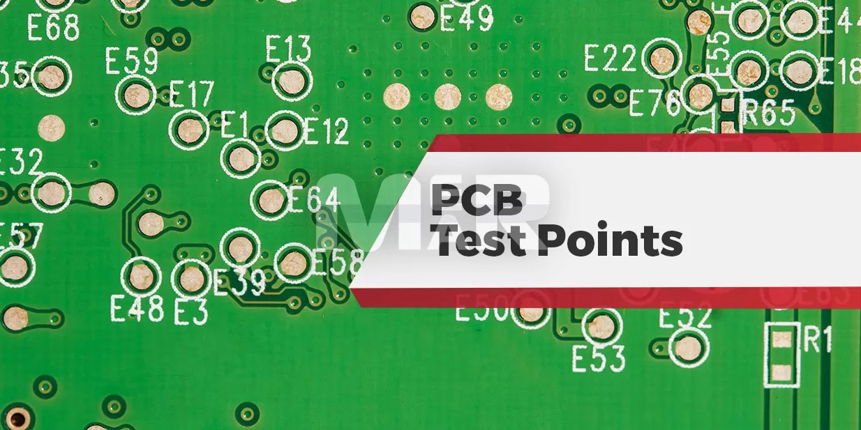
Verifying circuit functionality during development is critical for any electronic product. PCB test points serve as essential access nodes that allow engineers to inject signals and monitor board performance. At DYC Electronic, we integrate these verification features early in the PCBA prototyping phase to prevent costly failures later. This guide covers every technical aspect of implementation to help you optimize your next design. Understanding Verification Access Nodes A PCB test point is typically a small wire loop or exposed metal pad. Engineers use it to inject test signals and monitor the board’s circuitry directly. Comparing the output against desired results enables optimal design adjustments. These points must reside on the outer layer of the board for […]
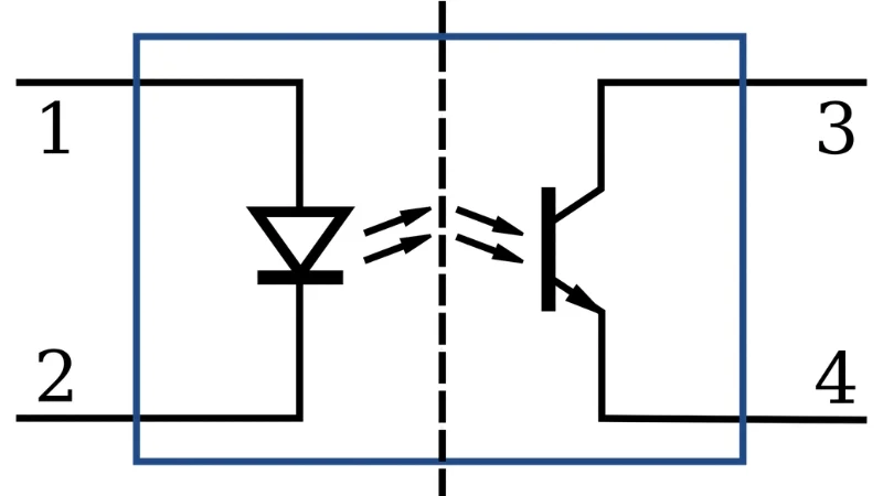
The 4N35 optocoupler remains a cornerstone in electronic manufacturing even in 2025. Despite newer digital isolators entering the market, this classic 6-pin DIP part anchors isolation circuits in industrial controls, power supplies, and motor drives. For procurement teams and design engineers alike, understanding its internal structure, operating modes, and critical specifications ensures reliable production outcomes. This guide covers everything from fundamental working principles to practical PCBA sourcing strategies. What Is the 4N35 Optocoupler and How Does It Work? The 4N35 optocoupler is a galvanic isolation component that transmits electrical signals between two isolated circuits using light as the medium. Specifically, an infrared LED (Light Emitting Diode) faces a silicon phototransistor […]

 日本語
日本語  English
  Русский
  Français
  Deutsch
  한국어
한국어  Español
  Português
  العربية
  Türkçe
  Italiano
  Polski
  Dansk
Dansk