
An unpopulated substrate equipped with copper traces, vias, pads, and dielectric layers serves as the fundamental carrier for nearly all electronic equipment. From consumer gadgets to high-performance aerospace systems, medical instruments, and industrial control devices, the bare PCB quality control process determines the final product’s success. Fabrication involves high-precision procedures like lamination, drilling, plating, imaging, etching, solder mask coating, and surface finishing. Each step introduces risks of defects such as broken traces, hidden shorts, uneven plating, or interlayer delamination. If defective boards reach assembly, they cause signal disorders, hardware failures, and safety hazards. Therefore, comprehensive testing is crucial to ensure performance, yield rates, and long-term reliability.
Full-Process Bare PCB Quality Control Workflow
Effective management of unpopulated boards operates as a closed-loop system spanning raw material input, on-site production monitoring, and pre-mass production verification. This systematic approach prevents defects rather than merely detecting them at the end.
Incoming Material Inspection Protocols
Incoming material inspection acts as the first critical checkpoint in bare PCB quality control. All copper-clad laminates, prepregs, solder mask inks, and surface treatment chemicals must meet UL, RoHS, and appropriate IPC requirements. Technicians thoroughly check supplier certification documents and inspect copper foil thickness uniformity. Additionally, they verify substrate flatness and surface conditions. Any materials that fail qualification or show contamination face immediate rejection, eliminating quality risks at the source. For detailed material specifications, refer to the IPC-4101 Laminate Standard.
Business Value Highlight: Rigorous incoming material inspection directly reduces costly rework and scrap rates during later production stages. By validating raw materials against UL and IPC standards upfront, procurement teams avoid supply chain disruptions and ensure consistent batch quality, ultimately protecting project timelines and profit margins.
In-Process Monitoring and First Article Inspection
Continuous in-process sampling tracks critical production steps throughout fabrication. Technicians manage drilling accuracy and burr size while monitoring etching precision to prevent copper residue or short circuits. Maintaining a dust-free workshop with stable temperature and humidity prevents pollution and pattern distortion on high-density fine-line multilayer boards. Furthermore, formal mass production always follows First Article Inspection (FAI). Teams completely measure the first completed boards dimensionally and electrically, comparing all data against original design drawings. Batch production commences only after parameters are fully adjusted and validated.
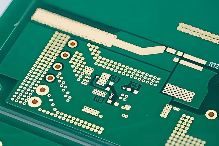
Core Testing Methods for Bare PCB Quality Control
Once fabrication concludes, complementary testing technologies verify surface appearance, electrical functions, and internal structural integrity. These methods form the backbone of reliable unpopulated board inspection.
Automated Optical Inspection (AOI)
After etching and solder mask processes, manufacturers extensively use Automated Optical Inspection (AOI). This technology combines high-resolution cameras with intelligent image comparison algorithms. AOI automatically detects visible defects like trace breaks, solder mask misregistration, surface scratches, missing copper, and residual copper shorts. Consequently, it effectively overcomes human visual fatigue limitations during prolonged inspection sessions.
Electrical Continuity Verification Testing
Verifying open and short circuits remains the most important functional test within PCB fabrication testing. Two mainstream modes exist for electrical continuity verification:
- Flying Probe Testing: Ideal for prototype development or small batch orders where circuit designs change frequently. It offers flexibility without custom tooling costs.
- Bed of Nails Testing: Best suited for large-volume mass production with fixed circuit designs. It provides faster testing speeds for high-throughput manufacturing.
Destructive Analysis and Surface Finish Verification
When non-destructive detection proves insufficient, technicians analyze internal defects through microsections and cross-section analysis per IPC-TM-650 Test Methods Manual. They cut and polish board samples, examining them under microscopes to verify lurking issues like plating voids, inconsistent via copper thickness, interlayer delamination, and multilayer misalignment. Simultaneously, surface finish inspection prevents solderability problems caused by oxidation on ENIG, HASL, or OSP finishes. For high-speed radio-frequency boards, impedance testing reduces signal attenuation and distortion during transmission.
Business Value Highlight: Implementing both flying probe and bed-of-nails testing strategies allows buyers to optimize costs across product lifecycles. Flying probe minimizes NRE expenses for prototypes, while bed-of-nails maximizes throughput for volume runs. This flexibility ensures you never overpay for testing regardless of order quantity.
IPC Standards Governing Bare PCB Quality Control
All circuit board reliability assurance adheres to global IPC specifications, primarily IPC-A-600 for visual acceptance and IPC-6012 for rigid board performance. Based on application needs, boards fall into three reliability classes:
| Class Level | Application Scope | Reliability Requirement |
|---|---|---|
| Class 1 | Consumer Electronics | Low demand, general function |
| Class 2 | Commercial/Industrial | Standard performance, extended life |
| Class 3 | Aerospace/Medical/Auto | High reliability, zero failure tolerance |
Testing devices undergo regular calibration, and complete sample test batch records remain available for customer review and audit. This ensures full quality traceability.
The Shift Toward Intelligent Digital Inspection
As electronics shrink and circuits become finer, traditional methods struggle to detect micro-defects. The industry is moving toward intelligent digital inspection. AI algorithms now enhance AOI recognition accuracy and reduce false judgment rates. Digital quality management platforms analyze real-time production data to predict parameter deviations, shifting inspection from passive defect screening to proactive risk prevention. Moreover, integrated multi-functional testing machines combine appearance, electrical, and dimensional detection, improving overall factory efficiency.
Strict bare PCB quality control and systematic testing guarantee qualified manufacturing. Every inspection link intercepts potential defects, levels out batch consistency, and satisfies international requirements from raw material testing to finished board verification. Engineers and enterprises seeking standardized, high-precision boards with complete testing records can rely on comprehensive solutions.
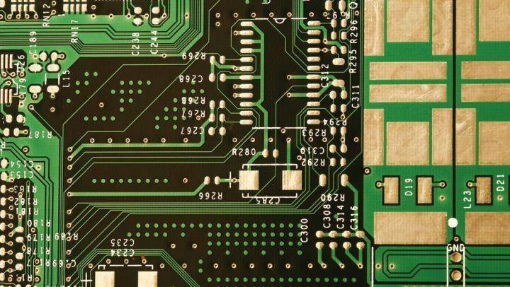
Frequently Asked Questions About Bare PCB Quality Control
What are the primary industry standards governing bare PCB quality control?
Quality control and testing strictly follow global IPC specifications. IPC-A-600 defines visual acceptance criteria, while IPC-6012 establishes performance requirements for rigid boards. Compliance with these standards ensures consistency across different manufacturers and applications.
How do manufacturers distinguish between Class 2 and Class 3 PCB reliability?
Class 2 covers commercial and industrial equipment requiring standard performance and extended life. Class 3 applies to aerospace, medical, and automotive safety hardware demanding high reliability and zero failure tolerance. Testing rigor and acceptance criteria increase significantly for Class 3.
When should I choose flying probe testing over bed-of-nails testing?
Select flying probe testing for prototype development or small batches with frequent design changes, as it avoids fixture costs. Choose bed-of-nails testing for large-volume mass production with fixed designs to achieve faster cycle times and lower per-unit testing costs.
What internal defects can cross-section analysis detect that AOI cannot?
Cross-section analysis reveals hidden internal issues such as plating voids, inconsistent via copper thickness, interlayer delamination, and multilayer misalignment. AOI only detects surface-level visible defects like trace breaks or solder mask misregistration.
How does AI improve modern automated optical inspection accuracy?
AI algorithms enhance AOI by learning from vast defect libraries, significantly reducing false judgment rates compared to traditional rule-based systems. This improvement increases true defect detection while minimizing unnecessary manual reviews, boosting overall inspection efficiency.
 日本語
日本語  English
  Русский
  Français
  Deutsch
  한국어
한국어  Español
  Português
  العربية
  Türkçe
  Italiano
  Polski
  Dansk
Dansk