
Bare PCB Quality Control: A Practical Guide to Testing and Reliability
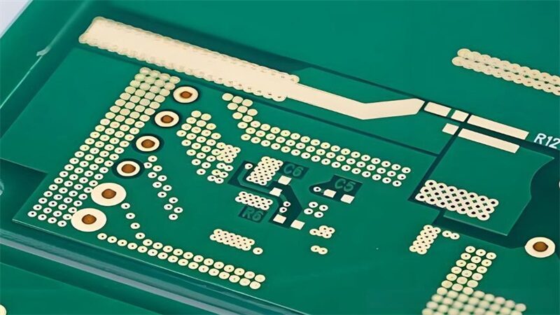
An unpopulated substrate equipped with copper traces, vias, pads, and dielectric layers serves as the fundamental carrier for nearly all electronic equipment. From consumer gadgets to high-performance aerospace systems, medical instruments, and industrial control devices, the bare PCB quality control process determines the final product’s success. Fabrication involves high-precision procedures like lamination, drilling, plating, imaging, etching, solder mask coating, and surface finishing. Each step introduces risks of defects such as broken traces, hidden shorts, uneven plating, or interlayer delamination. If defective boards reach assembly, they cause signal disorders, hardware failures, and safety hazards. Therefore, comprehensive testing is crucial to ensure performance, yield rates, and long-term reliability. Full-Process Bare PCB Quality Control Workflow […]
 日本語
日本語  English
  Русский
  Français
  Deutsch
  한국어
한국어  Español
  Português
  العربية
  Türkçe
  Italiano
  Polski
  Dansk
Dansk