
A board passes design review. The paste prints, and a 0.4 mm QFP bridges on three pins. The QFN center pad traps flux gas and voids at 35 percent. None of this shows up in the schematic. It starts at the steel sheet that lays down the solder. SMT stencil design is the discipline that sets how much paste lands on every pad. It also decides first-pass yield before the oven heats up. This article gives the rules we work to on every new job.
Short answer up front: size the foil to the finest pitch, hold the area ratio at 0.66 and the aspect ratio at 1.5, shrink apertures about 10 percent, and window-pane every QFN pad. Those four moves fix most print defects.
What Does SMT Stencil Design Control?
Short answer: it sets the volume and placement of solder paste on every pad, which drives more than 60 percent of all SMT defects. Good design prevents bridging, tombstoning, and voids before reflow.
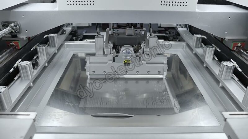
A stencil is a thin steel sheet with laser-cut openings. A squeegee pushes paste through those openings onto the pads. The thickness of the sheet sets the paste height. The shape of each opening sets how much paste each pad receives. Get either wrong, and the joint fails at reflow even when the placement machine and the oven are perfect.
In practice, this is where most yield loss starts. Industry data shows that over 60 percent of SMT assembly defects trace back to the print step. The stencil is the cheapest tool to fix and the most overlooked. Our IPC A-610 Class 3 guide covers how we judge the joint after reflow, but the stencil decides whether that joint forms at all.
The Two Ratios That Govern SMT Stencil Design
Short answer: two ratios predict paste release. Keep the area ratio at or above 0.66 and the aspect ratio at or above 1.5. Below those marks, paste sticks to the wall instead of dropping to the pad.
Area ratio equals the opening area divided by the wall area:
Area ratio = (L × W) ÷ [2 × (L + W) × T]
Aspect ratio equals the opening width divided by the foil thickness:
Aspect ratio = W ÷ T
| Ratio | Formula | Minimum |
| Aspect ratio | W ÷ T | 1.5 |
| Area ratio | (L × W) ÷ [2 × (L + W) × T] | 0.66 |
For square and rectangular openings, the area ratio is the binding limit, so check it first. A 0.25 mm square opening in 0.12 mm foil gives an area ratio of 0.52. That fails. Drop to 0.08 mm foil and the same opening reaches 0.78, which prints. A nano-coated sheet relaxes the area ratio floor to about 0.50. For 01005 parts, push the aspect ratio to 1.8. The rules come from IPC-7525, the stencil design guideline that most shops follow. IPC publishes both IPC-7525 and J-STD-005, which classifies paste by powder size.
How to Choose Stencil Thickness in SMT Stencil Design
Short answer: let the finest pitch on the board set the thickness, then use aperture shaping for everything coarser. Most industrial work lands on 0.10 mm or 0.12 mm foil.
Start from the tightest package, not the average part. However, a stencil sized for the connectors bridges every fine-pitch lead, and no squeegee tweak recovers it. The table below gives a working starting point:
| Smallest part | Pitch | Foil thickness |
| 01005, 0201 | 0.4 mm and under | 0.08 to 0.10 mm |
| 0402, 0.5 mm BGA | 0.5 mm | 0.10 to 0.12 mm |
| 0603 to 1206 | 0.8 to 1.0 mm | 0.125 to 0.15 mm |
| QFN, connectors | large pads | 0.15 to 0.20 mm |
Standard foils come in 0.08, 0.10, 0.12, 0.15, and 0.20 mm. Fine-pitch BGA and 01005 passives need the thin end. Power devices and RF shields on the same board need the thick end. When one sheet cannot serve both, a step stencil bridges the gap. Board flatness also matters, because a warped panel lifts away from the steel and starves the print. Our PCB bow and twist guide covers the flatness side of that problem.
Aperture Shapes by Package: SMT Stencil Design Rules
Short answer: shrink chip apertures about 10 percent, use home-plate shapes for gull-wing leads, keep BGA apertures round at 1:1, and split any QFN thermal pad into a window-pane.
One global rule starts every job: pull about 10 percent off the width of rectangular chip apertures. That keeps the foil sealed to the pad instead of riding up on the laminate edge. Beyond that, each package family needs its own shape.
| Package | Aperture shape | Key rule |
| Chip 0402 and larger | Rectangular, 10% narrower | Keep full length |
| 0201, 01005 | Square-end, 15 to 20% narrower | Never round the corners |
| QFP, SOIC | Home-plate | Reduce width 10 to 15%, round corners |
| BGA, CSP | Circular, 0.9 to 1.0× pad | Stay 1:1 below 0.5 mm pitch |
| QFN thermal pad | Window-pane grid | Target 50 to 70% of pad area |
The QFN center pad causes the most pain. A single open square floods the pad and traps flux gas, driving voids past 30 percent. Splitting it into a grid of 0.5 to 1.0 mm strips cuts voids below 10 percent, under the IPC 25 percent Class 3 limit. X-ray inspection confirms the void map on first-article builds.
Laser-Cut vs Electroformed Stencils: Which SMT Stencil Design Needs
Short answer: laser-cut stainless steel covers most boards down to 0.4 mm pitch, while electroformed nickel wins for ultra-fine pitch below 0.4 mm where wall smoothness sets release.
Laser cutting rules the mainstream. It cuts 304 or 316 stainless steel fast, ships in 24 to 48 hours, and lasts 50,000 to 100,000 prints at a low price. The wall finish after cutting is rougher, around 0.8 to 1.5 µm, so most shops add electropolishing to smooth it. Electroforming plates nickel atom by atom, reaching wall roughness of 0.1 to 0.3 µm. That smoothness lifts transfer efficiency and supports apertures down to 0.04 mm, but it costs two to three times more and needs five to seven days. ALLPCB publishes a fine-pitch comparison that shows where the trade turns in nickel’s favor.
A nano-coating adds a sub-micron hydrophobic layer to either type. It lifts paste release by 5 to 20 percent and roughly doubles the wipe interval. Framed stencils hold tension for automated lines; frameless stencils suit prototype and manual printing. New foil should hold tension at or above 35 N/cm, and at least 30 N/cm after wear.
Step Stencils in SMT Stencil Design
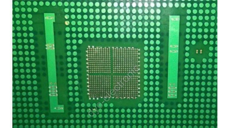
Short answer: a step stencil carries two or more foil thicknesses in one sheet, thinned in fine-pitch zones or raised under parts that need more paste. Pick one when the board mixes tiny and large parts.
Two forms exist. A step-up stencil thickens the areas with large connectors or through-hole pins, often from a 0.10 mm base to 0.15 mm. A step-down stencil thins the fine-pitch zones, often from 0.15 mm to 0.10 mm. The step depth usually sits between 0.02 and 0.05 mm. Go deeper and the squeegee blade takes damage.
Place the step away from fine-pitch parts. A hard edge near a 0.4 mm QFP prints unevenly and buries the benefit. Most shops cut the step by laser welding, chemical etching, or micro-machining, then electropolish the result.
How to Verify SMT Stencil Design Before Production
Short answer: SMT stencil design verification starts at the first article. Print the first five boards, measure every aperture with SPI, X-ray the BGAs, and set a clean schedule. Re-cut when transfer variance climbs past 10 percent.
Solder Paste Inspection (SPI) measures height, volume, and bridging on the first article. Run it on the first five boards of every build, not just the first build of the year. X-ray the first-article BGAs for a void map, and cross-section a new QFN design in-house the same day. Hold a sign-off before the line releases.
Cleaning keeps the print honest. Wipe the underside automatically every five prints on fine-pitch boards, every ten otherwise. A laser-cut stencil typically lasts 50,000 to 100,000 prints, while electroformed foil can reach 200,000. Fine-pitch sheets wear faster, so inspect the aperture edges weekly under a microscope. Any visible nick retires the sheet. Our incoming quality control page pairs this with the receiving checks we run.
Common SMT Stencil Design Mistakes
Short answer: 1:1 apertures, one open square on a QFN pad, a thickness set by the connectors, and missing fiducials. Each one shows up as a repeat defect, not a one-off.
- Accepting 1:1 apertures. A 1:1 opening bleeds paste under the foil and bridges fine-pitch leads. Always start from a 10 percent width reduction.
- One square on a QFN thermal pad. It floods the pad and voids the joint. Segment it into a window-pane at 50 to 70 percent coverage.
- Thickness set by the biggest part. A thick foil for a connector bridges every fine-pitch lead. Therefore, size the foil to the finest pitch, then shape the rest.
- No fiducials on the stencil. The printer cannot register without them. Add two global fiducials on opposite corners.
- Skipping the paste type check. Narrow apertures need finer powder. Match Type 3, 4, or 5 paste to the smallest opening, and keep the narrowest aperture about five particles wide.
FAQ
What stencil thickness should my board use?
Size the foil to your finest pitch. Use 0.10 to 0.12 mm for 0402 parts and 0.5 mm pitch, drop to 0.08 mm for 0201, 01005, or sub-0.4 mm parts, and raise to 0.15 to 0.20 mm for connectors and power devices. A step stencil handles boards that mix both.
What is a home-plate aperture?
A home-plate, or inverted trapezoid, shape for gull-wing leads. It narrows the aperture about 10 to 15 percent at the toe and heel while keeping full length. The wider gap between deposits cuts bridging on QFP and SOIC leads.
Why split a QFN thermal pad into a window-pane?
A single open square traps flux gas and drives voids past 30 percent. A grid of 0.5 to 1.0 mm strips lets the gas escape and cuts voids below 10 percent, under the IPC Class 3 limit of 25 percent.
When do I need a step stencil?
When one board carries fine-pitch parts that need a thin foil and connectors or through-hole pins that need a thick one. The step sets different thicknesses in one sheet, with a step depth of 0.02 to 0.05 mm.
How long does an SMT stencil last?
A laser-cut stainless stencil runs 50,000 to 100,000 prints, and an electroformed nickel stencil can reach 200,000. Fine-pitch sheets wear faster, so watch aperture edges and re-cut when transfer variance climbs past 10 percent.
Can I use one stencil for both board sides?
Rarely. Top and bottom sides usually carry different parts, pads, and paste volumes, and often need different foil thicknesses. Plan separate stencils for production, and keep frameless versions for prototype runs.
The Bottom Line on SMT Stencil Design
In the end, SMT stencil design decides yield before reflow. Size the foil to the finest pitch, hold the area ratio at 0.66 and the aspect ratio at 1.5, cut apertures about 10 percent, and window-pane every QFN pad. Those moves remove most print defects at the cheapest possible step.
Our SMT floor runs 6 Yamaha YS series lines and 6 AOI stations under ERP material control, with SPI on first-article builds.
Talk to Spancer Huang on WhatsApp +86 15818610980 or email info@dyc-electronic.com for a free stencil DFM review. Send us your paste Gerber and the finest pitch on the board. We will redline the apertures before we cut the steel.
 日本語
 English
 Русский
 Français
 Deutsch
 한국어
 Español
 Português
 العربية
 Türkçe
 Italiano
 Polski
 Dansk