
Preserving a solid IC local ground plane beneath high-speed processors is one of the most effective ways to suppress EMI at the source. A 0.5 mm pitch BGA sits on your top layer, and a critical clock trace needs to reach a connector on the opposite side. Do you route directly underneath the package body to save space, or do you maintain an unbroken copper zone? This decision defines whether your board passes EMC testing or becomes a radiating antenna.
In our builds, we have seen boards fail CISPR 32 Class B limits specifically because designers routed sensitive signals beneath noisy chips. Actually, the fix was not adding more ferrite beads. It was restoring proper grounding and moving the offending traces outside that keep-out zone. Here is what ten years of layout review taught us about this deceptively simple rule.
Why Unbroken Copper Prevents EMI Coupling
High-speed digital components generate significant electromagnetic interference during switching transitions. When signal traces pass directly beneath the package, they couple capacitively and inductively to internal die activity. This coupling injects noise onto otherwise quiet nets and turns those tracks into unintentional antennas.
Furthermore, routing under the component body complicates rework and debugging. Probe access becomes nearly impossible once the part is soldered down. In practice, technicians cannot clip oscilloscope probes to buried vias or inner-layer features hidden beneath a 27×27 mm BGA. Design for testability demands keeping the area under large devices accessible or at least predictable.
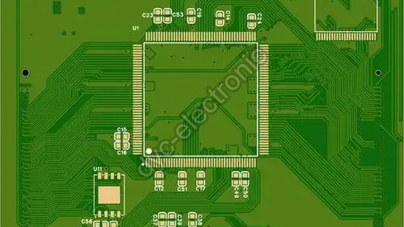
The 6.35 mm Extension Rule Explained
The original guidance from Wu Chuanbin’s 2015 technical note specifies a concrete dimension: the main ground pour must extend at least 1/4 inch (6.35 mm) beyond the package outline on all sides. This buffer zone serves two purposes. First, it ensures return current has a low-impedance path that does not fringe into adjacent signal layers. Second, it provides physical separation between the noisy device volume and any peripheral routing channels.
Consequently, when calculating keep-out zones, measure from the outermost pin or pad edge—not the silkscreen outline. Silkscreen tolerances can vary ±0.1 mm, while electromagnetic fields follow exact physics. That said, if board real estate makes the full 6.35 mm extension impossible on one side, prioritize extending toward the nearest high-speed connector or clock source. Partial coverage still outperforms zero coverage for your IC local ground plane.
Eliminating Island Copper Beneath Fine-Pitch Packages
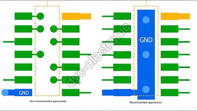
Fine-pitch QFN and BGA footprints create a persistent problem: top-layer pours between pads often form isolated islands that lack DC connection to the reference layer. These floating regions act as patch antennas at specific resonant frequencies determined by their geometry, undermining the entire shielding strategy.
To eliminate this risk, stitch every isolated region to the main ground using multiple vias. Place them at intervals no greater than λ/20 at the highest harmonic frequency of concern—typically 3–5 mm spacing for sub-6 GHz designs. Importantly, avoid placing vias so densely that they compromise solder mask dams between pads. A balanced approach uses 0.3 mm drills with 0.6 mm pads, spaced 4 mm apart in a grid pattern.
Engineer’s Note: Never leave top-layer pour under a BGA unconnected “just in case.” Floating copper causes more failures than it prevents. If you cannot stitch it reliably, remove it entirely and rely on the internal reference layer.
When Routing Through the Keep-Out Zone Is Unavoidable
Sometimes mechanical constraints force traces through the protected area. Heat sinks, mounting holes, or enclosure bosses may block all alternative paths. When this happens, apply three mitigation strategies simultaneously to protect your IC local ground plane integrity:
- Route only low-frequency, non-sensitive signals (e.g., GPIO, enable lines); never place clocks, RF, or differential pairs there.
- Insert a solid reference layer immediately below the routed traces to provide continuous return path and shield against vertical coupling.
- Add grounded guard traces on both sides of the signal, stitched with vias every 5 mm, to contain field spread.
These measures do not equal the performance of an unbroken copper zone, but they reduce risk to acceptable levels when zero-routing is physically impossible. Document every exception in the design review checklist so future revisions can address root-cause layout issues rather than applying band-aids.
Verifying Ground Integrity Before Fabrication
Before releasing Gerbers, run a DRC check specifically targeting connectivity under all devices >10 mm in size. Most EDA tools offer “island copper” or “dead copper” detection rules; enable them and set the minimum area threshold to 0.5 mm². Additionally, perform a visual inspection in 3D viewer mode to confirm via barrels actually connect through all layers—manufacturing misregistration can break intended connections even when netlist shows continuity.
For high-volume production, request impedance and TDR verification coupons that include ground via structures identical to those under critical components. This validates that your PCB ground pour strategy translates correctly from simulation to fabricated hardware. At high-speed PCB assembly facilities, we routinely cross-section these coupons to confirm plating quality before committing to full-panel processing. If your team lacks in-house DFM expertise, professional PCB layout services can catch these issues before tape-out.
Frequently Asked Questions About Ground Plane Sizing
What is the minimum recommended size relative to the package?
The established guideline requires the IC local ground plane to extend at least 6.35 mm (1/4 inch) beyond the package boundary on all sides. For devices larger than 20 mm, consider increasing this margin to 8–10 mm to account for higher total switching current and associated field spread.
The established guideline requires the IC local ground plane to extend at least 6.35 mm (1/4 inch) beyond the package boundary on all sides. For devices larger than 20 mm, consider increasing this margin to 8–10 mm to account for higher total switching current and associated field spread.
Can I route power traces through the protected zone if ground exists on another layer?
Technically yes, but it remains suboptimal. Power tracks carry switching noise that couples vertically through dielectric. Even with an intervening reference layer, dV/dt transients can induce displacement currents. Reserve the space directly under high-speed chips exclusively for ground; route power rails around the perimeter instead.
Technically yes, but it remains suboptimal. Power tracks carry switching noise that couples vertically through dielectric. Even with an intervening reference layer, dV/dt transients can induce displacement currents. Reserve the space directly under high-speed chips exclusively for ground; route power rails around the perimeter instead.
How does via stitching density affect effectiveness at different frequencies?
At frequencies below 1 GHz, 5 mm spacing typically suffices. Above 3 GHz, reduce spacing to 2–3 mm to prevent cavity resonance between the top pour and internal layer. Always model the specific stackup; FR4 dielectric constant and thickness determine actual resonant modes. Generic rules fail when layer count exceeds eight.
At frequencies below 1 GHz, 5 mm spacing typically suffices. Above 3 GHz, reduce spacing to 2–3 mm to prevent cavity resonance between the top pour and internal layer. Always model the specific stackup; FR4 dielectric constant and thickness determine actual resonant modes. Generic rules fail when layer count exceeds eight.
Final Recommendations for Reliable High-Speed Layout
Preserving an IC local ground plane is not optional for modern high-speed designs—it is foundational EMC hygiene. The 6.35 mm extension rule, aggressive island copper elimination, and disciplined routing exceptions together form a defense-in-depth strategy that survives both lab validation and field deployment.
If your current layout team treats ground pours as afterthoughts or leaves fine-pitch areas un-stitched, expect intermittent failures that no amount of post-layout filtering will fix. Get ahead of these issues with a professional layout review focused specifically on return path management.
Ready to validate your next high-speed design? Send us your preliminary files for a free DFM and grounding integrity assessment. We’ll identify island copper risks, insufficient via stitching, and routing violations before you commit to fabrication.
 English
  Русский
  Français
  Deutsch
  日本語
日本語  한국어
한국어  Español
  Português
  العربية
  Türkçe
  Italiano
  Polski
  Dansk
Dansk