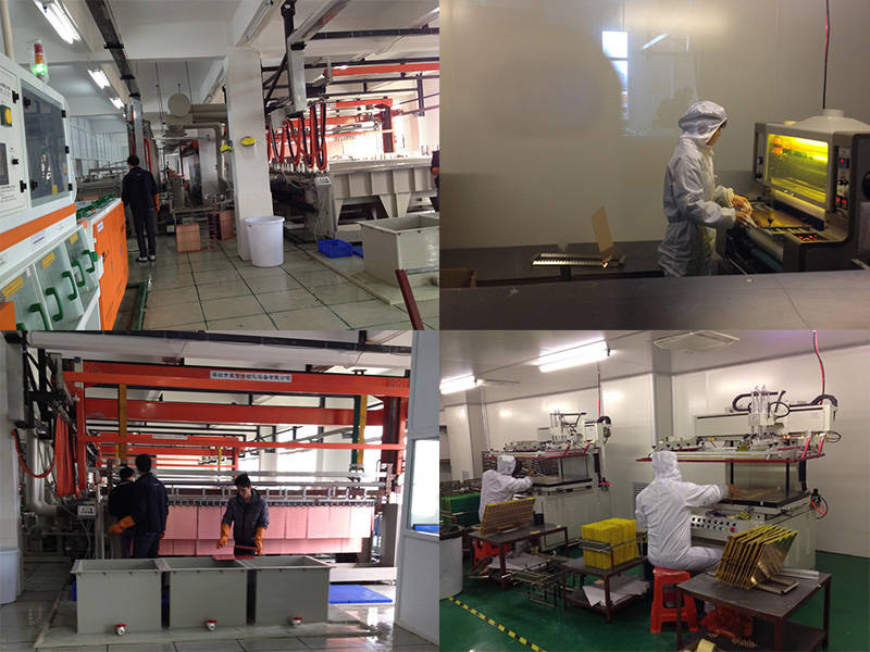
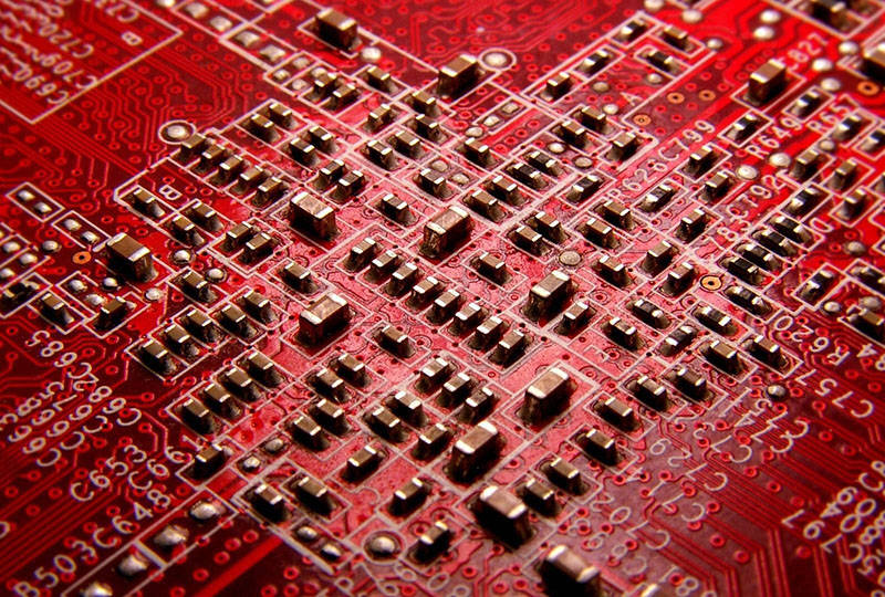
DYC Electronic has a full technical knowledge and PCB manufacturing experience in PCB fabrication (also called printed circuit board manufacturing or printed circuit board fabrication). From single layer board to 32 layer board, from flex PCB to rigid-flex PCB, DYC can offer the complete PCB solution.
PCB Prototype
1-32 Layer PCB Prototype for Rigid, Flex and Rigid-Flex board, we offer 24 hours Quick Turn PCB prototype.
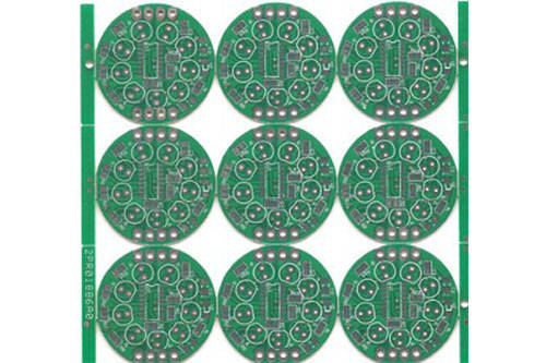
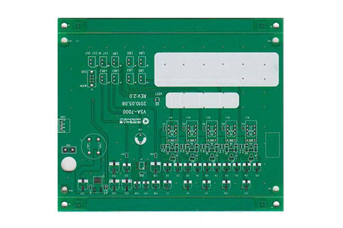
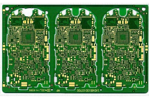
Rigid PCB
From single layer to 32 layers rigid printed circuit board with no minimum order requirement.
Impendence Control PCB
We offer free impedance control calculations suggestions for your controlled impedance PCB.
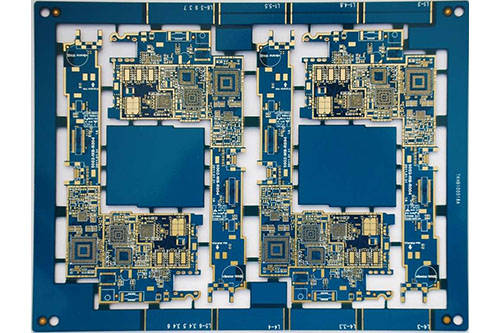
HDI PCB
HDI PCBs offers higher circuitry density per unit so that can make your device more portable.
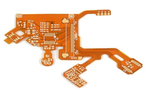
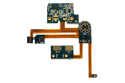
Flexible PCB
We produce 1-4 layers flexible Printed circuit board from fabrication and assembly.
Rigid Flex PCB
A circuit board made by combining hard and soft boards to reduce connectors and increase the reliability of interconnections
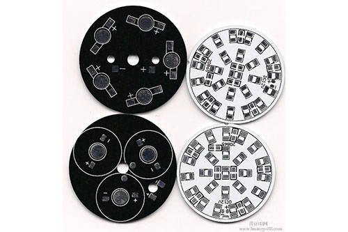
Aluminum PCB
Our 1-6 layers aluminum PCB fabrication will give you best performance and low-cost solution.
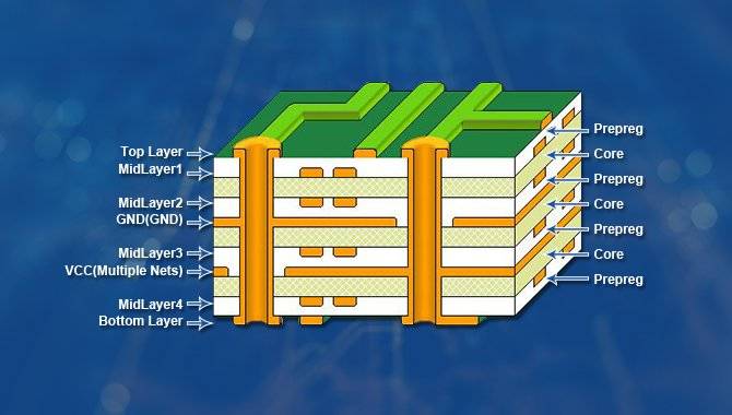
DYC: Your Leading Layer Stack-up Supplier in China
DYC Layer Stackup is the basic process to avoid emission, crosstalk, and all other kinds of disturbances of high-speed applications.
There is really no limit to the number of layers that can be fabricated in a multilayer PCB, and DYC’s maximum capability is 32 layers.
Most of the boards we are building every day are less than 16 layers. To find out more about multilayer boards layer stack-up information, please feel free to contact our sales.
We also offer free stack-up checking, you are more than welcome to contact us.
Over 10 years’ experience
Highly trained and skilled engineers
Cost-effective PCB layer stackup
Fast turnaround
What is PCB Layer Stackup?
Our team focused on optimal multilayer stack-up because it is one of the most important factors in determining the EMC performance of a product.
For example, to improve the EMC performance of a 4 layer board, it is better to space the signal layers as close to the planes as possible and use a large core between the power and ground plane.
This is the most effective way to improve the performance of a 4 layer board. We can also balance well the Signal Integrity (SI) against manufacturability and reliability to have a good multilayer stack up.
PCB layer stackup is a way to getting multiple printed circuit boards in the same device by stacking them on top of each other while making sure there is a predefined mutual connection among them.
Important 4 tips before pcb layer stackup design
Tip #1: Determining the Number of Layers
This includes consideration of signal, power and grounding layers or planes. It is highly recommended that you do not mix signal types on the inner layers.
Tip #2: Determine the layer arrangement
Route high speed on microstrip of minimum thickness.
There should be a minimum spacing between the power and ground layers.
Tip #3: Determine layer material type
Another important consideration for PCB stackup is the thickness of each signal layer. This should be determined along with determining the thickness of the prepreg and core material.
Tip #4: Determine routing and vias
Completing the PCB laminate design is the determination of the alignment and routing. This includes determining the weight of the copper, where to place the vias, and what type of vias to implement.
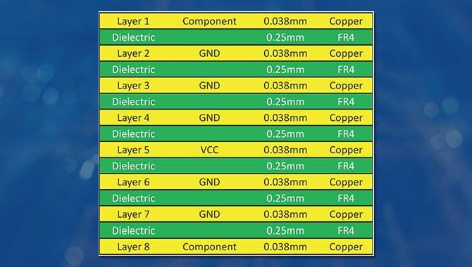
what is Power and ground layers in the layer stackup and its advantage
The power layer is the copper layer connected to the power supply. It is usually designated as VCC in PCB designs. The main function of the power layer is to provide a stable voltage supply to the PCB. Similarly, the grounding layer is a flat copper layer connected to a common ground point in the PCB.
Advantages of using a power/grounding layer
The component‘s power and ground pins can be easily connected to the power and ground planes. It provides a clear path for current return, especially for high-speed signals. This, in turn, reduces EMI (electromagnetic interference).
The current carrying capacity of the power supply layer is larger than that of the alignment. The operating temperature of the PCB also can be reduced.
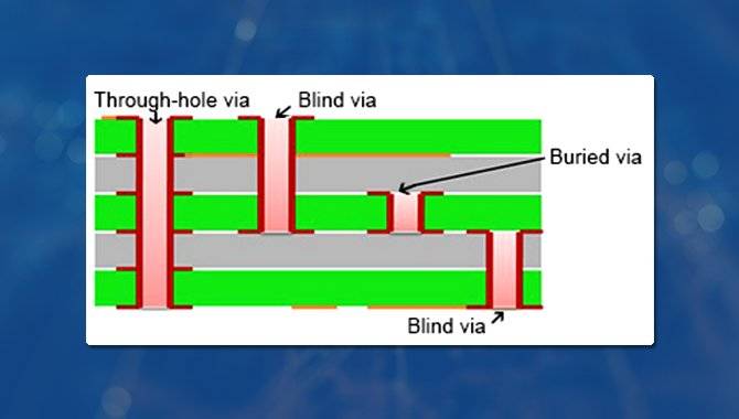
Blind and Buried Vias Layer stackup
Our team focused on optimal multilayer stack-up because it is one of the most important factors in determining the EMC performance of a product.
For example, to improve the EMC performance of a 4 layer board, it is better to space the signal layers as close to the planes as possible and use a large core between the power and ground plane.
This is the most effective way to improve the performance of a 4 layer board. We can also balance well the Signal Integrity (SI) against manufacturability and reliability to have a good multilayer stack up.
Certifications & Compliance
DYC Electronic has established a comprehensive technology research and development system.
✔ CCC certification ✔ ISO9001:2015 system certification ✔ ISO14001:2015 system certification ✔ ISO13485:2016 system certification ✔ IATF16949 system certification ✔ Supply chain management system ✔ MES process traceability system ✔ Environmental management system