
A 0402 capacitor sits 2 mm from the board edge. During SMT assembly, the conveyor rail clamps down and crushes it before reflow even starts. This happens more often than you’d think. In our builds, we see this failure when designers treat the PCB process edge design as an afterthought rather than a first-order constraint. The fix isn’t expensive, but catching it late costs real money in rework and delayed shipments.
This guide walks through the exact margins, mark points, and separation methods that keep boards running smoothly on high-speed SMT lines. No theory dumps—just the parameters we verify during every DFM check.
Why SMT Rail Clearance Defines Your PCB Process Edge Design
SMT machines use paired rails to transport boards through stencil printing, pick-and-place, and reflow zones. Those rails need physical space to grip without touching components or solder paste. That reserved strip is what we call the process edge, also known as the conveyor belt margin or breakaway rail.
Theoretically, most SMT equipment requires only 3.0 mm of bare substrate for clamping. Actually, designing to that absolute minimum invites trouble. Any slight misalignment or board warpage pushes components into the clamp zone. Consequently, we recommend 5.0 mm as the safe no-placement boundary for reliable PCB process edge design.
When components fall inside this forbidden zone, two bad outcomes follow. Either the assembler must hand-solder those parts after reflow, adding labor cost, or they must build custom fixtures to shield them. Both options inflate your unit price and extend lead time.
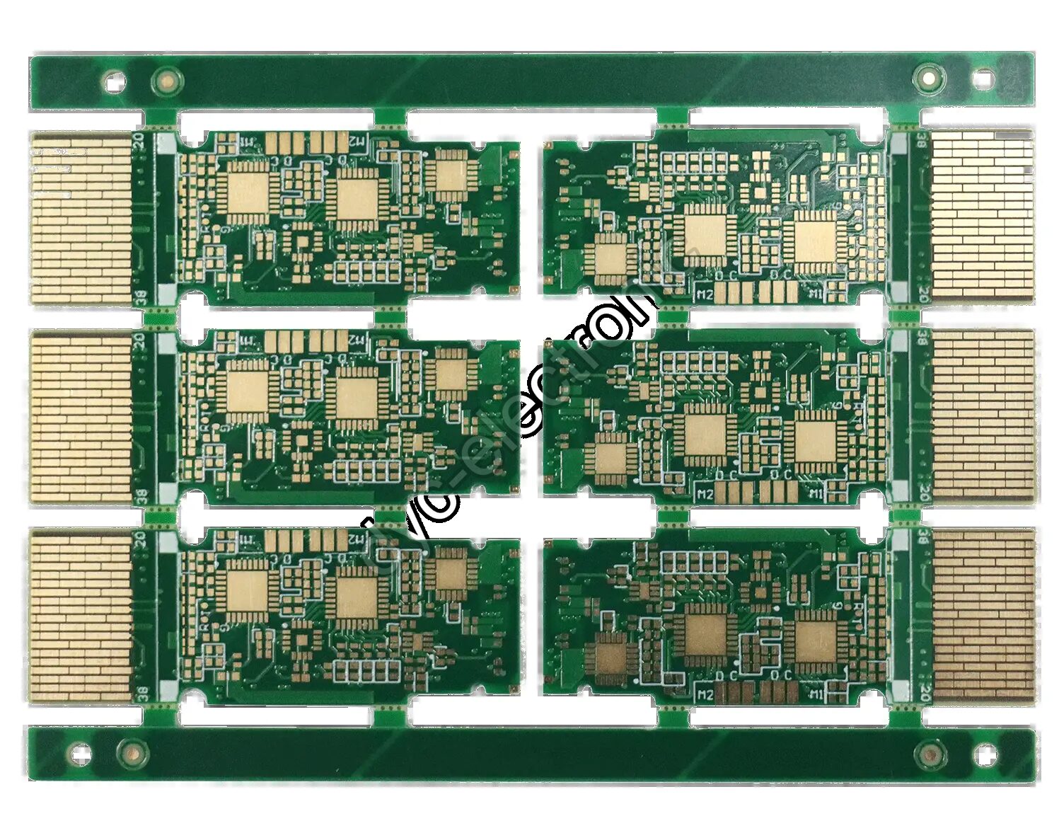
Engineer’s Note: If all SMDs already sit beyond the 5 mm boundary from both long edges, you may skip adding dedicated breakaway rails entirely. However, this is rare in dense designs. Always confirm with your assembler’s specific machine specs before waiving the rail.
Choosing Long Edge vs Short Edge Placement
Where you place the process edge affects both yield and cost. Adding rails to the longer sides increases total panel area, which raises the per-unit material cost. Yet it also lets the board enter the SMT machine lengthwise, providing better rigidity against nozzle pressure during placement.
Conversely, placing rails on the shorter sides saves material and lowers average cost per piece. The trade-off is reduced stiffness. Thin or large-format boards may flex under the placement head, causing misalignment or tombstoning. Here’s the catch: this approach only works when the base laminate has sufficient thickness-to-span ratio.
In practice, we default to long-edge rails for boards thinner than 1.0 mm or wider than 100 mm. For thicker, compact boards, short-edge rails are acceptable and more economical. Always validate stiffness by simulating or testing one sample panel before committing to volume.
Furthermore, the orientation decision impacts downstream processes like AOI and functional testing. Test fixtures often assume a consistent entry direction. Align your PCB process edge design choice with the entire assembly flow, not just placement.
Fiducial Marks and Tooling Holes in Breakaway Rails
SMT vision systems rely on fiducial marks for precise alignment. If your active circuit area lacks adequate marks, you must add them to the process edge itself. Typically, two to four diagonal fiducials provide sufficient redundancy for multi-camera systems.
Standard fiducial diameter is 1.0 mm with exposed copper and solder coating. Make sure the surrounding solder mask opening is at least twice the pad diameter for reliable optical recognition. When board-internal marks exist and meet spacing requirements, extra rail marks become optional—but never assume. Verify camera field-of-view coverage with your assembler first.
Additionally, tooling holes serve dual purposes. They locate the panel during fabrication routing and electrical test, and they assist automated handlers during assembly. We specify three to four plated-through holes per rail, nominally 3.0 mm in diameter. This size offers the best balance between locating precision and structural integrity.
Critically, these holes must be non-plated if used solely for mechanical registration, or plated if serving as ground vias. Mixing up this detail causes drill breakout or poor clamping. Specify clearly on the fabrication drawing.
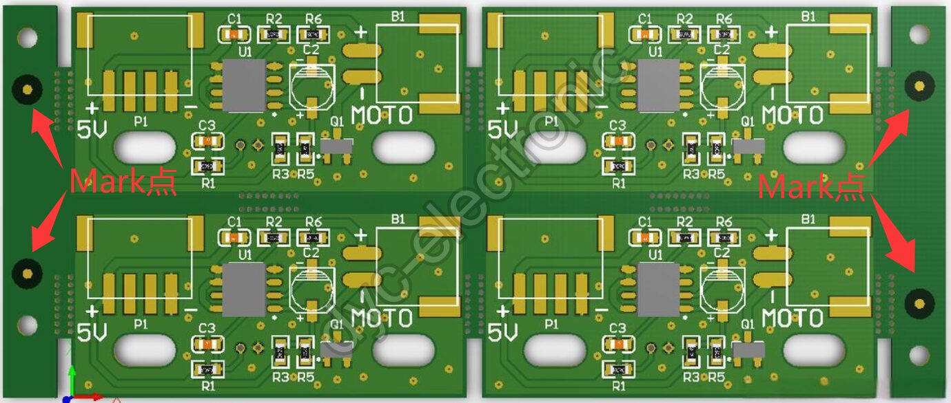
Procurement Tip: Ask your PCBA supplier whether their SMT line uses global or local fiducial correction. Global-only systems demand stricter mark placement tolerance (±0.05 mm), while local systems tolerate ±0.1 mm. Matching your PCB process edge design to their capability avoids costly respins.
Separation Methods: V-Score vs Stamp Hole Tabs
After assembly, individual boards must separate cleanly from the panel. Two dominant methods exist: V-groove scoring and perforated tab routing (stamp holes). Each suits different product profiles.
V-scoring cuts a shallow groove along straight lines, leaving about one-third of laminate thickness intact. It produces clean, straight edges ideal for rectangular boards with no cutouts near the separation line. Moreover, V-score panels depanelize quickly with minimal stress on nearby components when done correctly.
Stamp hole tabs use small drilled bridges connecting board to rail. They allow irregular outlines and curved separations that V-scoring cannot achieve. However, depanelizing introduces higher mechanical shock. Components within 3 mm of the tab risk cracking, especially brittle MLCCs. Therefore, maintain adequate standoff distance or switch to V-score whenever geometry permits.
On the other hand, some hybrid designs combine both methods. Use V-score for primary separation and tabs only where contours force it. This balances edge quality with geometric flexibility. Always specify residual web thickness for V-scores (typically 0.4–0.6 mm depending on board thickness) to prevent premature snapping during handling.
Critical Keepout Zones and Copper Rules Inside Process Edges
The process edge is not free real estate for random copper features. Strict keepout rules protect both assembly reliability and operator safety.
First, no SMD or auto-inserted through-hole components may reside inside the rail or extend above it. Hand-inserted THT parts have limited vertical clearance: maximum 3.0 mm above top/bottom rails and 2.0 mm above left/right rails. Exceeding these limits risks collision with clamps or sensors.
Second, copper traces within the rail should be wide and robust. Traces narrower than 0.4 mm require additional insulation and abrasion protection due to repeated rail contact. Outermost traces must be at least 0.8 mm wide to withstand mechanical wear over multiple production cycles.
Third, avoid placing pads or vias directly in the clamp zone. Solder residue or plating buildup creates uneven surfaces that compromise clamping force. Over time, this leads to board slippage and placement drift.
Finally, any single board exceeding 80 mm² must include its own pair of parallel process edges unless integrated into a larger panel with shared rails. This ensures independent support during bench handling and inspection.
Field Lesson: We once saw a batch fail AOI because flux residue accumulated on narrow rail traces, creating false shorts. Widening outer traces to 1.0 mm and adding solder mask dams eliminated the issue permanently. Small PCB process edge design tweaks like this save big headaches later.
Frequently Asked Questions About PCB Process Edge Design
What is the minimum recommended width for PCB process edge design in SMT assembly?
While 3.0 mm is the theoretical equipment limit, we strongly advise 5.0 mm as the practical minimum for PCB process edge design. This extra margin accommodates board warpage, fixture tolerances, and prevents component interference during clamping. Designs using exactly 3.0 mm frequently require post-assembly rework.
Do I always need to add fiducial marks on the process edge?
Not necessarily. If your active area already contains properly spaced and sized fiducials visible to the SMT camera system, rail-mounted marks are redundant. However, when internal marks are absent or poorly positioned, adding two to four diagonal fiducials on the process edge becomes mandatory for accurate SMT assembly alignment.
Should I choose V-score or stamp hole tabs for panel separation?
Choose V-score for straight-line separations on rectangular boards—it yields cleaner edges with less mechanical stress. Reserve stamp hole tabs for irregular outlines or curved boundaries. Never place fragile components within 3 mm of tab locations. Hybrid approaches combining both methods often deliver optimal results for complex PCB panelization design rules.
Can I omit the process edge if components are far from the board edge?
Yes, provided all SMDs and sensitive features sit outside the 5 mm conveyor belt margin on both long sides. Confirm this with your assembler’s specific equipment specifications before proceeding. Even then, consider retaining minimal rails for handling convenience during testing and packaging. Skipping PCB process edge design entirely saves cost but increases handling risk.
Final Thoughts on Reliable PCB Process Edge Design
Getting the PCB process edge design right upfront prevents costly line stoppages and rework downstream. Maintain 5 mm rail clearance, position fiducials strategically, select appropriate separation methods, and enforce strict keepout zones. These aren’t optional best practices—they’re baseline requirements for smooth SMT assembly.
Ready to validate your next design? Send us your Gerber files for a free DFM review focused specifically on process edge compliance and assembly yield. Our engineers will flag clearance violations, mark point gaps, and separation risks before you commit to fabrication.
 English
  Русский
  Français
  Deutsch
  日本語
日本語  한국어
한국어  Español
  Português
  العربية
  Türkçe
  Italiano
  Polski
  Dansk
Dansk