
A stack of bare boards arrived flat, passed incoming checks, and then bowed after the first lead-free reflow. The BGA coplanarity failed, the placement head scraped a panel, and the line stopped for two hours. PCB bow and twist is the measurement that catches this before it happens: for any board carrying surface-mount parts, IPC-A-600 caps it at 0.75%. The root cause is almost never bad luck — it is copper imbalance or an asymmetric stack-up, and the fix starts at layout, not in the reflow oven.
Short answer up front: keep flatness at 0.75% or less for SMT boards, 1.5% for through-hole-only boards, measured per IPC-TM-650 Method 2.4.22. Design a mirror-symmetric stack-up, balance copper across layers, and control the reflow ramp — those three moves prevent most of the warpage we see.
What Are PCB Bow and Twist?
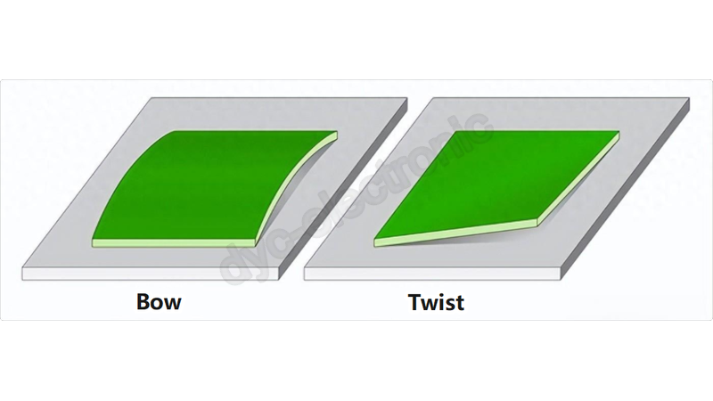
Short answer: they are the two flatness characteristics IPC-A-600 §2.11 defines. Bow is a roughly cylindrical or spherical curvature where all four corners still sit in the same plane. Twist is deformation parallel to the diagonal, where one corner leaves the plane of the other three.
Put a board on a flat table. If the middle rises while all four corners stay down, that is bow. Press one corner down; if the opposite corner lifts, that is twist. Both are physical measurements converted to a percentage, never a visual impression. Per IPC-A-600 §2.11, bow and twist are determined by physical measurement and percentage calculation in accordance with IPC-TM-650 Method 2.4.22.
Two rules trip people up. First, the percentage is relative to the board’s own dimensions, so a 100 mm board and a 300 mm panel fail at very different absolute deflections. Second, panels that are assembled in panel form and later separated are assessed in panel form, not as individual boards — measuring after depaneling hides the problem that actually broke your line.
What Are the IPC Limits for PCB Bow and Twist?
Short answer: 0.75% for boards using surface-mount components and 1.50% for all other boards, acceptable across Class 1, 2, and 3. In practice, high-density builds need far tighter internal limits, because reflow adds deformation after the bare board passed.
The calculation is straightforward. Bow percentage equals maximum bow height divided by board length, times 100. Twist percentage equals maximum corner lift divided by the diagonal length, times 100. So a 200 mm board with 1.0 mm of bow reads 0.50%, and a 250 mm diagonal lifting 1.5 mm reads 0.60% twist.
| Application | Typical limit | Basis |
| SMT boards | ≤ 0.75% | IPC-A-600 §2.11 / IPC-A-610 §10.2.6 |
| Through-hole-only boards | ≤ 1.50% | IPC-A-600 §2.11 |
| BGA / fine-pitch PCBA | ≤ 0.50% or tighter | Customer-specific, common in practice |
| Recommended IQC internal limit | ≤ 0.50% | Reflow adds 30–50% warpage |
| Automotive / military high-reliability | ≤ 0.30% | Contract-specific |
Critically, the bare-board number is not the number your line experiences. Third-party labs commonly see warpage grow 30–50% through reflow, and one supplier’s data on ultra-thin boards shows 0.3% after fabrication rising to 0.8% after a single lead-free cycle. That is why an IQC gate at 0.50% rather than 0.75% is the safer default. The same 0.75% maximum carries into assembly workmanship: IPC expert panels note that IPC-A-610 §10.2.6 references the identical limit measured the same way, and IPC-6012 sets the qualification criteria behind it.
What Causes PCB Bow and Twist?
Short answer: an imbalance in how each half of the board wants to expand. Copper runs a coefficient of thermal expansion near 17 ppm/°C against roughly 14–16 ppm/°C for FR-4, so any asymmetry in copper, stack-up, or material turns heat into curvature.
Uneven copper distribution is the most common driver. A large ground pour on one layer facing sparse traces on the next creates a modulus and CTE mismatch that flexes the board the moment it heats. Unbalanced stack-up is the second: specifying 3 oz copper on one layer of a four-layer board and 1 oz on the rest all but guarantees warpage. Prepreg grain orientation matters too, because fiberglass strands under tension should alternate direction between dielectric layers rather than run parallel through the stack. Mixed materials such as a Rogers/FR-4 hybrid behave the same way, since each side contracts differently on cooling.
Process and environment add to the design-driven stress. Moisture absorbed in storage vaporizes in the preheat zone and bulges the board from inside. Reflow peak temperature above the laminate’s Tg lets residual stress relax and reshape the panel, and double-sided SMT accumulates that deformation across two cycles. Rapid cooling after hot-air leveling or plating, uneven etching, and drill smear residue all contribute. Thin, large panels amplify every one of these effects.
How to Prevent PCB Bow and Twist in Design
Short answer: make the top half a mirror of the bottom half, then equalize copper where routing density differs. Symmetry is the single most effective fix, and it costs nothing but layout discipline.
The most effective structure is a mirror-symmetric stack-up around the center plane. Layer N from the top must match layer N from the bottom in copper weight, core thickness, prepreg type, and resin content. Use an even layer count, keep dielectric thickness and foil type identical in mirrored positions, and hold prepreg resin content consistent. Where routing density genuinely differs, balance it deliberately rather than leaving it to chance.
- Copper balancing — target roughly 40% copper fill on every layer, and hold the imbalance between mirrored pairs within about ±10%.
- Thieving patterns — add electrically isolated dummy copper in open areas to equalize plating and etching current density.
- Grid fill over solid pour — cross-hatch a ground plane instead of flooding it, which cuts local copper density without losing the return path.
- Panel layout — center the board array, add copper-balance borders, and avoid mixing very different copper densities in one panel.
- Material selection — match CTE across core and prepreg, prefer high-Tg laminates, and avoid odd layer counts.
Engineer’s Note: Copper balancing is not free. Dummy copper near signal traces changes capacitance and can shift impedance, so on high-speed and RF boards balance with grid patterns and verify with simulation rather than flooding open space.
How to Control PCB Bow and Twist in Fabrication and Assembly
Short answer: control the thermal ramp everywhere, bake out moisture before reflow, and support the panel while it is soft. Warpage is created by temperature change, so every degree-per-minute you remove is deformation you never have to rework.
In fabrication, the lamination recipe dominates. Published process guidance specifies a heating ramp of 2–3 °C per minute, a gel-point hold of roughly 15–20 minutes for uniform wetting, and cooldown of 2–3 °C per minute under pressure until the panel drops below Tg all reduce locked-in stress. For thick boards above 2.0 mm or builds beyond twelve layers, a post-lamination stress-relief bake at 150 °C for two to four hours, done before drilling, pays for itself. Store panels vertically in racks rather than stacked, because horizontal creep adds its own flatness error.
In assembly, three controls matter. Bake moisture-sensitive boards per IPC/JEDEC J-STD-033 before reflow so trapped water cannot pop them open. Soften the profile, following published ultra-thin guidance of a ramp of 2 °C per minute or less up to 150 °C, a 60–90 second soak between 150 °C and 180 °C, and a peak of 245 °C maximum for SAC305 with 40–60 seconds above liquidus. Then support the panel in a pallet or carrier during reflow and let it cool before removal, because a board above Tg has almost no rigidity. Boards on mixed-material stacks benefit from seven to ten heating zones with the slowest ramp the schedule allows.
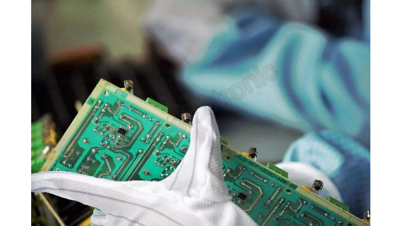
Post-reflow measurement closes the loop. A 3D profilometer or laser scan on sampled boards catches the drift that incoming inspection cannot, and shadow moiré interferometry reveals transient warpage at reflow temperature — the state that actually breaks BGA coplanarity. Pair this with a controlled reflow profile rather than adjusting the profile after the damage is done.
A Practical Checklist for PCB Bow and Twist Control
Short answer: run the checks at three points — design release, bare-board incoming, and post-reflow. Five steps cover most of the exposure. Ultimately, flatness is cheapest to secure before the panel ever enters an oven.
- Review the stack-up for mirror symmetry and even layer count at design release.
- Run a copper-area analysis per layer and flag any mirrored pair beyond roughly 20% imbalance.
- Measure bow and twist on incoming bare boards per IPC-TM-650 2.4.22, in panel form, against a 0.50% internal limit.
- Record the values by lot and trend them, since a slow drift signals a press or plating change before it becomes a line stop.
- Verify post-reflow warpage on sampled boards and reconcile any escape against the profile, the bake, and the fixture support.
Those incoming records belong in your incoming quality control file, because they are the evidence that separates a fabrication issue from an assembly-profile issue when a warp escape reaches the field.
FAQ
What is the acceptable PCB bow and twist limit?
For boards using surface-mount components, IPC-A-600 §2.11 sets bow and twist at 0.75% or less. All other boards may reach 1.50%. BGA and fine-pitch assemblies are commonly held to 0.50% or tighter by customer specification.
Why is my PCB warped after reflow when it arrived flat?
Reflow relaxes residual stress in the laminate, especially above Tg, and lead-free peaks of 245–260 °C make the resin mechanically soft. Labs commonly see 30–50% growth in warpage through reflow, and unbaked moisture can add localized bulging on top of it.
How do you calculate PCB bow and twist?
Bow percentage is maximum bow height divided by board length, times 100. Twist percentage is maximum corner lift divided by the diagonal length, times 100. Both are measured per IPC-TM-650 Method 2.4.22.
Does IPC-A-610 also cover bow and twist?
Yes. IPC-A-610 §10.2.6 references the same 0.75% maximum warpage, measured by the same IPC-TM-650 method, for assemblies carrying surface-mount components.
Conclusion
Overall, PCB bow and twist is a flatness problem with a small number of real causes and a clear numeric bar. Hold 0.75% for SMT boards and 1.50% for through-hole-only boards per IPC-A-600, but set your internal IQC limit nearer 0.50% because reflow adds 30–50% before the board reaches placement. Mirror the stack-up, balance copper within roughly ±10% between layers, bake out moisture per J-STD-033, and ramp the oven slowly — and warpage stops being a line-stop surprise.
At DYC Electronic, our ERP-managed process control, 6 Yamaha YS SMT lines, and 6 AOI stations let us measure bare-board flatness per IPC-TM-650 2.4.22 on every incoming panel and verify post-reflow warpage on sampled boards.
Talk to Spancer Huang on WhatsApp +86 15818610980 or email info@dyc-electronic.com for a free DFM review that checks stack-up symmetry and copper balance before your boards go to panel — and ask us to confirm the flatness spec on your purchase order.
 Türkçe
  English
  Русский
  Français
  Deutsch
  日本語
日本語  한국어
한국어  Español
  Português
  العربية
  Italiano
  Polski
  Dansk
Dansk