
Modern electronic devices demand smaller sizes, faster speeds, and greater functionality. Consequently, printed circuit board complexity has increased dramatically. Dense layouts with fine-pitch packages and thousands of solder joints make manual inspection inefficient and unreliable. Therefore, manufacturers rely on Automated Optical Inspection to guarantee production quality. This technology serves as a critical checkpoint in both fabrication and assembly processes.
What Is Automated Optical Inspection?
Automated Optical Inspection is a machine-based visual inspection method. High-resolution cameras, controlled lighting, and image processing software scan PCBs to detect defects automatically. The system captures board images and compares them against reference data like CAD files or golden boards. Any deviation signals potential manufacturing issues.
This technology applies across multiple production stages. During fabrication, it verifies structural integrity including trace patterns and pad conditions. In assembly, PCB defect detection focuses on component positioning and solder joint quality after surface-mount or through-hole placement. Manual methods simply cannot match this accuracy for complex designs.
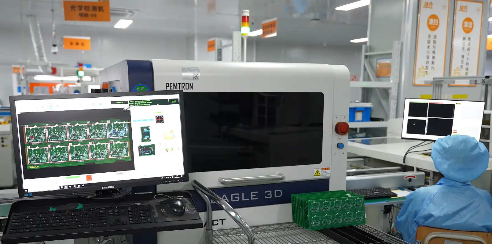
Furthermore, AOI provides fast, cost-effective inspection for large-scale production runs. It ensures quality consistency that human operators cannot maintain over extended periods.
How Machine Vision Inspection Works
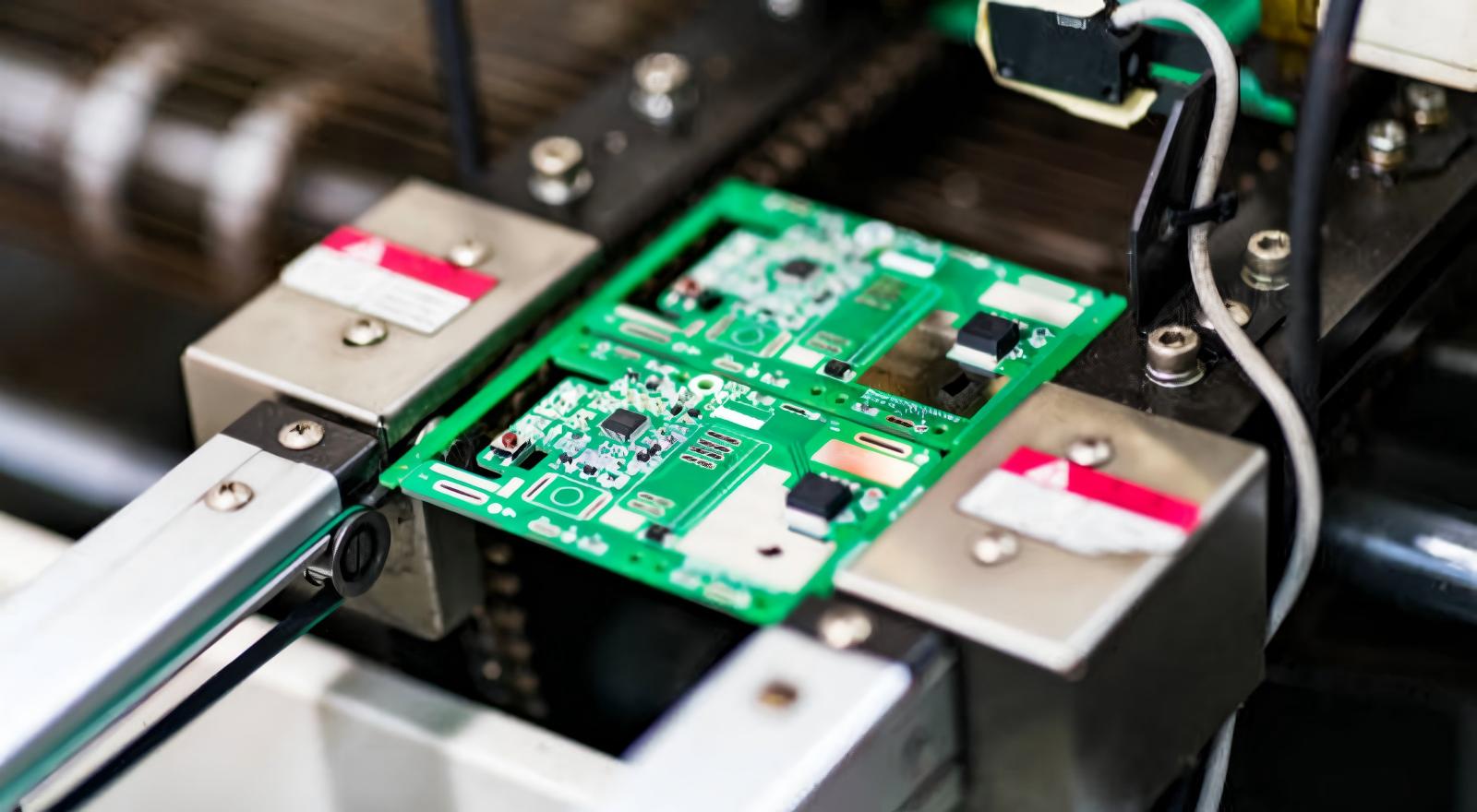
Advanced machine vision inspection systems combine intelligent software with precision hardware. An automated conveyor first feeds the PCB into the AOI machine. High-resolution cameras then capture detailed images of components, solder joints, pads, and circuit traces.
Lighting plays a crucial role in inspection accuracy. Modern systems use programmable LED arrays that adjust angle and color to enhance contrast. Different lighting configurations highlight specific problems like solder bridges or component misplacement. For instance, angled illumination reveals height variations while diffuse lighting shows surface markings.
Subsequently, inspection software analyzes captured images for shape, dimension, and positional accuracy. The system compares current images against reference data to identify differences. Next-generation equipment achieves sub-pixel measurement accuracy, detecting microscopic anomalies that could cause electrical failures. When defects appear, the system flags them for operator review and logs inspection data for traceability.
Business Value Highlight: Implementing optical testing system technology reduces escape rates by identifying defects at the source. This real-time feedback loop prevents faulty boards from reaching downstream assembly stages, protecting your brand reputation and reducing warranty claims.
AOI Application Stages in PCB Manufacturing
Manufacturers integrate PCBA quality control at various points depending on inspection goals and cost considerations. Each stage targets specific defect categories.
During bare PCB fabrication, AOI checks for open circuits, short circuits, and improper trace widths. Spacing anomalies and missing pads are also detected. Identifying these issues early prevents defective boards from entering assembly lines.
Pre-reflow inspection occurs before soldering in assembly lines. This step verifies solder paste deposits and confirms correct component placement. Post-reflow solder joint verification assesses joint quality and component positioning after soldering. Since most assembly defects originate during reflow, this stage proves essential. Additionally, some manufacturers perform final AOI before shipment as a comprehensive quality gate.
Defects Detected by Automated Optical Inspection
Automated Optical Inspection systems identify diverse manufacturing and assembly errors quickly and consistently. Bare board inspection catches short circuits, open circuits, and line width violations. Excessive copper, surface scratches, contamination, and damaged vias are also flagged.
Assembly inspection detects missing, wrong, or misaligned components. Polarity errors, skewed parts, flipped components, and placement offsets are common finds. Moreover, the system identifies soldering defects including insufficient solder, excess solder, bridges, raised leads, tombstoning, and inadequate coverage. Early detection prevents costly repairs at later production stages.
| Defect Category | Bare PCB Examples | Assembly Examples |
|---|---|---|
| Electrical | Short/Open Circuits | Missing/Wrong Components |
| Physical | Trace Width Violations | Misalignment/Skew |
| Surface | Scratches/Contamination | Tombstoning/Raised Leads |
| Solder | Pad Integrity Issues | Bridges/Insufficient Solder |
Key Benefits of AOI in PCB Production
Adopting automated optical inspection delivers substantial advantages for modern fabrication. Superior inspection standards top the list. As components shrink, even minute positional errors cause failures. AOI systems find small variations impossible for human inspectors to detect reliably.
Cost reduction follows improved first-pass yield. Early defect identification saves rework expenses, material waste, and labor costs. Flexibility represents another major benefit. Since AOI inspects both fabricated boards and assembled PCBs, it applies across multiple production steps. Programmable lighting and adjustable parameters accommodate various board designs and finishes.
Additionally, inspection data collection enables process optimization. Engineers analyze defect trends, discover root causes, and refine manufacturing parameters. Consequently, overall efficiency improves continuously.
Why AOI Importance Continues Growing
The rising significance of automated optical inspection directly connects to PCB evolution. Fine-pitch components, high-density interconnect designs, and multilayer boards with microvias demand precision beyond human capability. A single PCB may contain thousands of solder joints where even tiny defect rates impact product reliability.
Consistent quality regardless of production scale eliminates operator fatigue and subjectivity variances. Furthermore, AOI enhances manufacturing efficiency through rapid feedback. Identifying defects early allows engineers to adjust fabrication or assembly parameters in real time. Thus, identical problems do not propagate to subsequent boards.
Complementary Inspection Methods
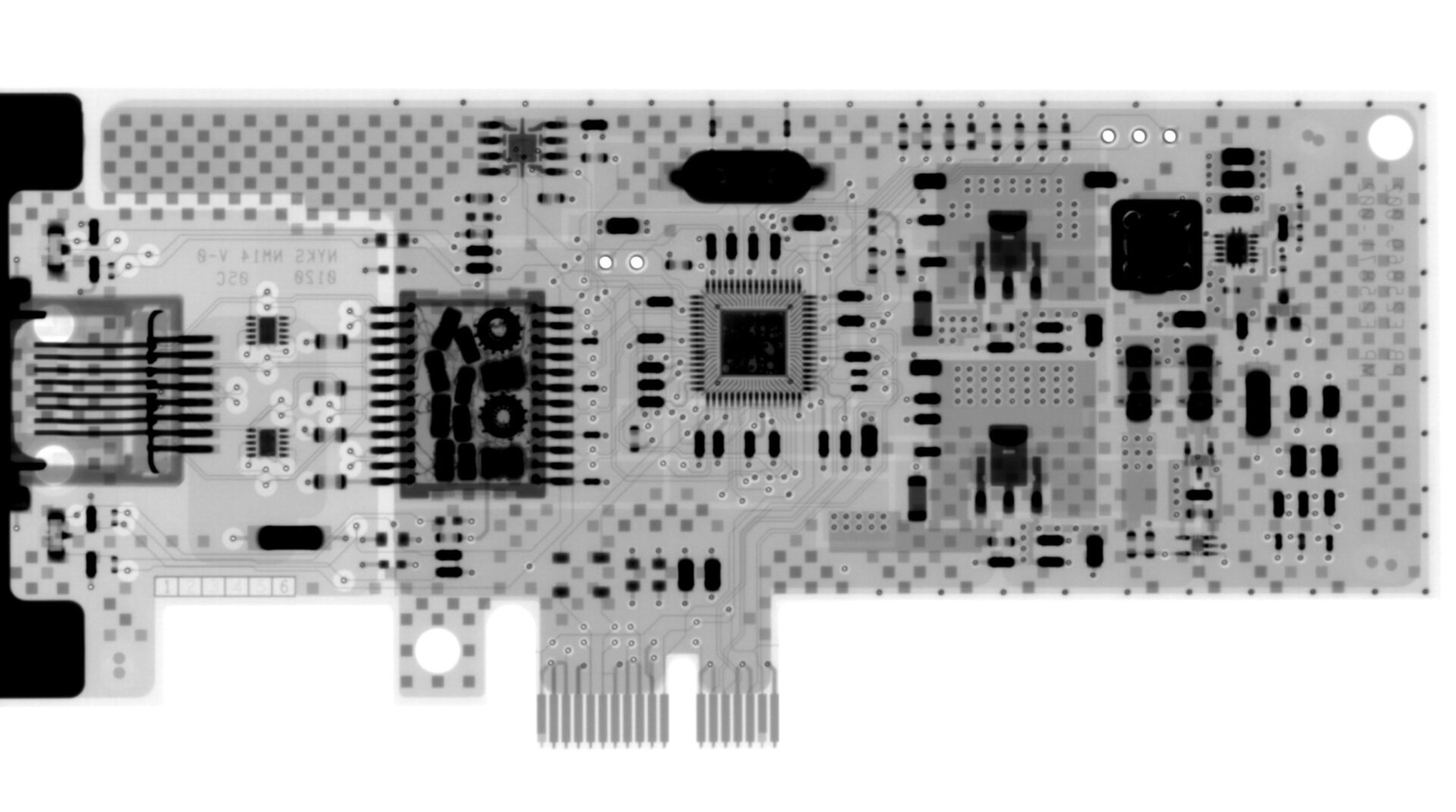
While automated optical inspection excels at visible defect detection, limitations exist. Hidden connections beneath BGA packages remain inaccessible to optical systems. Therefore, manufacturers typically combine AOI with X-ray inspection and electrical testing. This multi-modal approach verifies internal solder joints and circuit functionality comprehensively.
Integrating complementary techniques provides complete PCB quality assurance. Continuous inspection at critical fabrication and assembly steps enables real-time process control. Manufacturing teams detect deviations instantly and enforce strict quality standards throughout production. By combining advanced inspection with process optimization, suppliers deliver reliable PCBs for demanding electronic applications.
For professional PCB Assembly Services incorporating comprehensive AOI protocols, consult experienced manufacturers. Understanding these inspection capabilities helps buyers evaluate supplier quality commitments effectively. Explore our PCB Manufacturing Capabilities to learn more about integrated quality systems.
Frequently Asked Questions About AOI
1.Can Automated Optical Inspection detect all PCB defects?
No. While automated optical inspection identifies visible surface defects excellently, it cannot see hidden solder joints under BGA or QFN packages. Manufacturers supplement AOI with X-ray inspection for internal verification and functional testing for electrical validation.
2.At which production stages should AOI be implemented?
Optimal implementation includes post-fabrication bare board inspection, pre-reflow paste and placement verification, and post-reflow solder joint verification. Final pre-shipment inspection adds another quality layer. Stage selection depends on product complexity, volume, and acceptable risk levels.
3.How does AOI compare to manual visual inspection?
Machine vision inspection surpasses manual methods in speed, consistency, and defect detection capability for modern PCBs. Human inspectors suffer from fatigue and subjectivity, especially with fine-pitch components. AOI maintains consistent standards across high-volume production while capturing quantitative data for process improvement.
4.What reference data does AOI use for comparison?
Systems typically compare captured images against CAD design files or verified golden boards. CAD-based programming suits new product introductions, while golden board comparison works well for established production runs. Advanced systems combine both approaches for maximum PCB defect detection accuracy.
5.Does AOI slow down production throughput?
Actually, automated optical inspection increases effective throughput by catching defects early. Preventing faulty boards from progressing through expensive assembly stages saves overall cycle time. Modern inline AOI systems operate at conveyor speeds matching SMT line takt times without creating bottlenecks.
 Türkçe
  English
  Русский
  Français
  Deutsch
  日本語
日本語  한국어
한국어  Español
  Português
  العربية
  Italiano
  Polski
  Dansk
Dansk