In PCB layout design, the layout of components is crucial. It determines the neatness and beauty of the circuit board and the length and number of printed circuits, which has a certain impact on the reliability of the entire machine.
In addition to realizing the principle function, a good circuit board must also consider electrical characteristics such as EMI, EMC, ESD (electrostatic discharge), signal integrity, etc., as well as the mechanical structure and heat dissipation issues of high-power chips, ETC.
This article puts forward some suggestions for general PCB layout for your reference.
General PCB layout specification requirements
- Read the design documents to meet the layout requirements of special structures, special modules, etc.
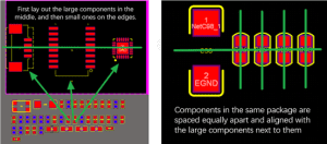
- Set the layout grid point to 25mil, which can be aligned according to grid points and at equal intervals; the alignment method is large first and then small (large devices and large devices are aligned first), and the alignment method is centered, as shown in the figure below.
- Meet the height limit of the prohibited area, the layout of the structure and special devices, and the requirements of the prohibited area.
1)As shown in Figure 1 below (left): the height limit requirements are clearly marked on the mechanical layer or marking layer to facilitate later cross-checking;
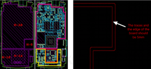
2)As shown in Figure 1 below (right): Set a prohibited area before layout, requiring devices to be 5mm away from the board edge. Do not lay out devices unless there are special requirements or process edges can be added in subsequent board designs;
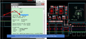
3)As shown in Figure 2 below: The layout of the structure and special devices can be accurately positioned by coordinates or positioned according to the component outer frame or centerline coordinates.
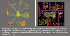
- The layout must be pre-layout first. Do not start the layout directly after getting the board. The pre-layout can be based on the analysis of the signal flow direction of the line drawing in the PCB board after grabbing the module, and then based on the signal flow analysis, on the PCB board Draw the module auxiliary lines inside, evaluate the approximate position and occupation range of the module in the PCB, draw the auxiliary lines with a width of 40 mil, and evaluate the rationality of the layout between modules through the above operations, as shown in the figure below.
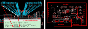
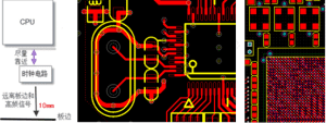
- The layout needs to consider the channels for power wiring, which should not be too tight. Through planning, you can also figure out where the power comes from and sort out the power tree, as shown in the figure below (left).
- When laying out heat-sensitive components (such as electrolytic capacitors and crystal oscillators), they should be placed as far away from high-heat devices as power supplies and as far upwind as possible, as shown in the figure below (right).
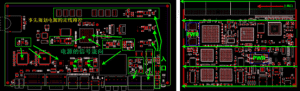
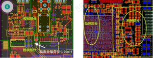
- Meet the distinction of sensitive modules, the balance of the entire board layout, and the reservation of wiring channels for the entire board, as shown in the figure below.
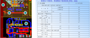
1)High-voltage and high-current signals are completely separated from small current and low-voltage weak signals. All layers of the high-voltage part are hollowed out. No additional copper is required. The creepage distance between high voltages should be checked according to the standard table. As shown below;
2)Analog signals and digital signals should be separated, with a separation width of at least 20mil, and analog and radio frequencies should be laid out in a ‘one’ shape or an ‘L’ shape according to the requirements in the modular design, as shown in the figure below (left);
3)Separate high-frequency signals from low-frequency signals, with a distance of at least 3mm, and no cross-layout, as shown in the figure below (right);
4)The layout of key signal devices such as crystal oscillators and clock drivers needs to be away from the interface circuit layout and not placed on the edge of the board. There must be a distance of at least 10mm from the edge of the board. Crystals and crystal oscillators are placed close to the chip and placed on the same layer. Do not drill holes. Reserve space for the land, as shown in the picture below;
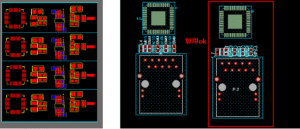
5)The circuits with the same structure adopt “symmetrical” standard layout (the same modules are directly reused) to meet the consistency of signals, as shown in the figure below.
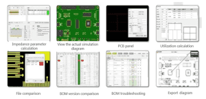
After designing the PCB, analysis and inspection must be done to make production smoother.