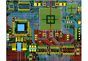
According to the PCB design process, after the PCB layout was completed, a rigorous review process is required to determine whether the designed product meets the ESD or EMI requirements. Excluding schematic design, PCB design generally required to review both layout and wiring. DYC Electronics will introduce EMC design suggestions for PCB layout.

EMC Design Layout Inspection Recommendations
- Suggestions for overall layout inspection
1) Analog, digital, power, and protection circuits should be separated, and there should be no overlap on the three-dimensional surface;
2) High speed, medium speed, and low speed circuits should be separated;
3) Strong current, high voltage, and strong radiation components should be kept away from small current, low voltage, and sensitive components;
4) Multi layer board design must have separate power and ground planes;
5) For heat sensitive components (including liquid electrolytic capacitors and oscillators), try to stay away from high-power components, heat sinks, and other heat sources as much as possible.
- Suggestions for interface and protection layout inspection
1) The sequence of general power supply lightning protection devices is: varistor → fuse → suppression diode → EMI filter → inductance or common mode inductance, and for any missing components in the schematic diagram, the layout should be extended accordingly;
2) The general order of protective devices for interface signals is: ESD (TVS transistor) → isolation transformer → common mode inductance → capacitance → resistance. For any missing components in the schematic diagram, a sequential layout is carried out;
3) The level conversion chip (such as RS232) should be placed close to the connector (such as the serial port);
4) Devices that are susceptible to ESD interference, such as NMOS and CMOS devices, should be kept as far away from areas that are susceptible to ESD interference (such as the edge area of a single board) as possible.
- Suggestions for checking clock circuit layout
1) The filter of the clock circuit (preferably using a “π” type filter) should be close to the power input pin of the clock circuit;
2) The layout of crystals, oscillators, and clock distributors should be kept away from high-power components, heat sinks, and other heating devices;
3) Crystals, oscillators, and clock dividers should be as close as possible to related IC devices;
4) The distance between the oscillator and the board edge and the interface device should be greater than 1 inch.
- Suggestion for checking the layout of switching power supply
1) Switching power supply should be kept away from AD/DA converters, analog devices, sensitive devices, and clock devices;
2) Strictly follow the requirements of the schematic diagram for PCB layout, and do not randomly place the capacitors of the switching power supply;
3) The PCB layout of the switching power supply should be compact, and the input/output should be separated.
- Suggestion for checking the layout of capacitors and filter components
1) In principle, each power pin should be placed with a 0.1uf small capacitor, and an integrated circuit should be placed with one or more 10uf large capacitors, which can be increased or decreased according to specific circumstances;
2) Capacitors must be placed close to the power pins, and capacitors with smaller capacitance values should be placed closer to the power pins;
3) The EMI filter should be close to the input port of the chip power supply.
- Suggestions for stack inspection
1) Multilayer boards (four or more layers) have at least one continuous and complete ground plane used to control the impedance and signal quality of the PCB;
2) Place the power supply plane and ground plane close to each other;
3) Try to avoid two signal layers being adjacent to each other as much as possible. If the distance between the two signal layers is increased, and the wiring should be misaligned and not overlapped. Otherwise, later wiring may cause crosstalk;
4) Avoid adjacent power supply planes, especially those caused by signal layer power supply laying;
- Other design inspection suggestions
1) When the entire machine is designed as a floating equipment, it is recommended not to design each interface separately;
2) When the machine casing is made of metal, the power supply is three holes, and it is required that the metal casing must be well connected to the ground.
