
A MOSFET on a 5 W buck converter runs fine on the bench. Bolt it into a sealed enclosure, however, and the same part climbs past 110 °C within minutes. PCB thermal management is what separates a board that survives field use from one that cooks its own solder joints. Actually, heat is not a side effect you fix later. It is a layout decision you make on layer one.
Why Your Board Overheats: The Heat Spreading Trap
Heat in a PCB follows one unglamorous equation: ΔT = P × R_th. Power dissipated times thermal resistance equals the temperature rise above ambient. Specifically, a 1 oz copper plane on FR-4 holds roughly 70 °C/W per square centimetre, so a 3 W part dumps a 200 °C rise onto a postage-stamp pad. Worse still, FR-4 itself conducts at only 0.3 to 0.4 W/m·K, about five times worse than the aluminium base in a metal-core PCB.
Engineer’s Note: Measure the pad temperature, not the case label. A component rated for 150 °C junction can still roast a nearby electrolytic cap. Thermal maths is only as good as the R_th you actually built.
Do You Even Need Thermal Vias?
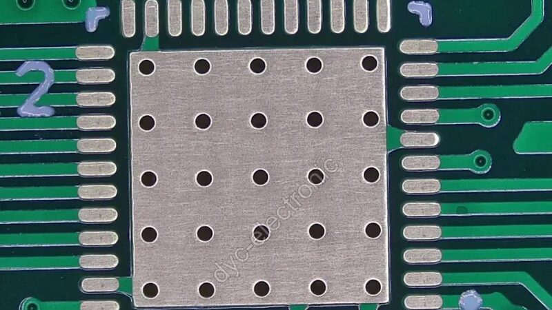
Not every board does. A 0.2 W logic IC shrugs off heat through its leads and the solder mask. But any package with an exposed pad (QFN, DPAK, TO-252, PowerSO) needs a real path down into the board. Thermal vias move heat vertically through the substrate into inner planes and the far side. In practice, that path is the only one a bottom-side exposed pad actually has.
Specifically, the via diameter should land at 0.3 to 0.5 mm with a centre-to-centre pitch of 0.8 to 1.5 mm. Shrink the pitch below 0.5 mm and the copper web between holes gets too thin to carry current or spread heat. Additionally, keep vias at least 0.15 mm inside the pad edge to avoid solder wicking.
Sizing the Thermal Via Array
One open via is almost useless. The plated barrel alone gives roughly 70 to 100 °C/W, so you need an array. Field data shows a 3×3 grid (9 vias, 0.3 mm, 1.0 mm pitch) under a 3 mm QFN lands near 35 °C/W, a 4×4 grid near 20 °C/W, and a 5×5 near 14 °C/W. Fill the vias with copper epoxy or solid copper and the per-via resistance drops to 20 to 45 °C/W, up to four times better than an empty hole.
Field Lesson: Voids kill arrays. Outgassing during reflow traps air under the pad, and air is a terrible conductor. Therefore, cut the solder-paste opening to 50 to 75 % of the pad with a windowed stencil, and target under 25 % X-ray voiding. One big void can wipe out 15 to 25 % of your thermal budget.
Copper Pours Spread Heat Sideways
Thermal vias handle the vertical path. Copper planes handle the horizontal one. A continuous inner plane at 80 to 90 % fill spreads heat across a wide, low-resistance sheet instead of a narrow hotspot. Push coverage past that, however, and the board warps in reflow from uneven copper stress, so keep the stackup symmetric. For extreme loads, a metal-core PCB swaps FR-4 for an aluminium base at 1 to 2 W/m·K.
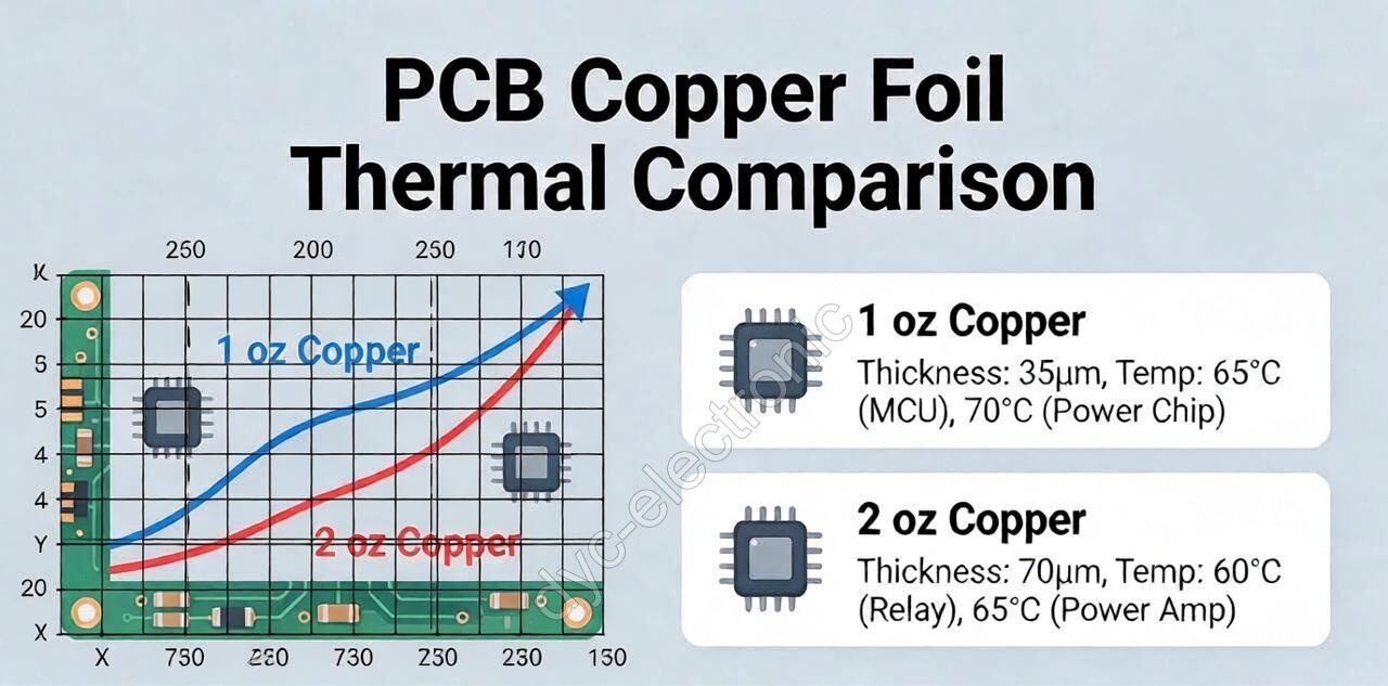
Copper weight sets how fast it spreads. In practice, switching the thermal layer from 1 oz (35 µm) to 2 oz (70 µm) roughly doubles lateral spreading and can cut a LED or MOSFET temperature by 10 to 20 °C for a 10 to 20 % cost bump. Three-ounce copper goes further still, though etching tolerances tighten.
The Relief Mistake That Breaks Thermal Vias
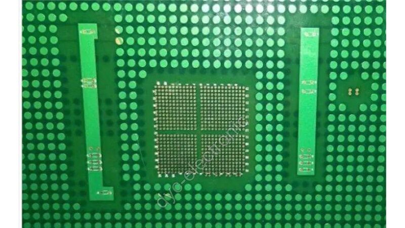
Here is the catch engineers miss. Thermal reliefs, those little spoke patterns, are for hand-soldered signal pins, not power pads. Put spokes on a thermal via and you add 2 to 5 °C/W of resistance per plane connection, choking the very path you built. Connect thermal vias with solid, direct copper to the plane instead. That said, a few designers still prefer relief for hand rework, which is a fair call on prototypes.
Procurement Tip: Ask the fab for solid-connect thermal vias and a 2 oz inner plane on power builds. A shop that buries “standard relief” in the default stack-up can hand you a board that fails thermal qualification. Spec it in the PO.
IPC-2152 and the Current-Carrying Capacity You Can Carry
Trace heating is the other half of PCB thermal management. IPC-2152, the standard for determining current-carrying capacity, replaced the old IPC-2221 single-formula approach with nomographs built from real multilayer boards. Its core relation is I = k × ΔT^0.44 × A^0.725, where k is 0.048 for outer layers and 0.024 for inner at a 20 °C rise. Notably, inner layers therefore need roughly twice the width for the same current.
For a 20 °C rise on 1 oz external copper, the charts give roughly: 1 A at 10 mil width, 3 A at 50 mil, 5 A at 100 mil, 10 A at 250 mil. Inner layers carry only about half that. Consequently, size the trace for your worst-case ambient and duty cycle, not the datasheet typical. A solid PCB layout design guide helps you place those wide traces early, before routing gets crowded.
Common Thermal Layout Mistakes
Most overheating traces back to a short list. First, the exposed pad floats with no vias, so the part cooks. Second, vias sit outside the pad, and heat never reaches the plane. Third, a single narrow trace carries the full load instead of a poured bus. Fourth, the designer forgets that inner layers run hotter and sizes them like outer ones.
A clean PCB layout design guide keeps copper away from break lines and pours it toward the heat. For extreme dissipation, a metal-core PCB swaps FR-4 for an aluminium base at 1 to 2 W/m·K. Pair either with a balanced PCB layer stack-up and the hotspot problem often disappears.
FAQ
How many thermal vias do I need under a QFN?
Start from the pad size. A 3 mm QFN wants a 3×3 array at 0.3 mm drill and 1.0 mm pitch (≈35 °C/W); a 7 mm part wants 5×5 (≈14 °C/W). Fill them with copper epoxy when the pad will be soldered, since empty vias wick solder and starve the joint.
Is 2 oz copper worth the cost for thermal management?
Usually yes. It roughly doubles lateral heat spreading and can drop component temperature 10 to 20 °C for a 10 to 20 % price increase. Above 5 W per part, 2 oz on the thermal layer should be your floor.
Can I use thermal relief on power pads to help soldering?
No. Relief spokes add 2 to 5 °C/W per plane and defeat the pad. Use a windowed stencil at 50 to 75 % paste coverage instead, and keep the via-to-plane connection solid.
Get a DFM Thermal Review Before Tooling
Good thermal layout is cheap insurance. In practice, most failures we see trace back to a missing via array or a floating pad. Before you release a power board, send us your stack-up and power map. We return a DFM thermal review that flags via count, copper weight, and plane continuity against your real load, free and usually within one business day.
We run thermal and assembly in a 5,000 m² plant with 300+ staff and 20+ R&D engineers, under an ERP-managed quality system . Our floor carries 6 Yamaha YS high-speed SMT lines, 6 automatic printers, 6 AOI units, 2 lead-free DIP lines, 2 conformal-coating lines, and 2 final-assembly lines, with annual capacity of 2 million finished units and 6 million PCBA boards. Contact Spancer Huang on WhatsApp +86 15818610980 or email info@dyc-electronic.com for a competitive quote or sample policy. Ultimately, pairing a metal-core PCB option with this PCB thermal management checklist is the fastest way to keep both the junction and the scrap rate cool.
 English
  Русский
  Français
  Deutsch
  日本語
日本語  한국어
한국어  Español
  Português
  العربية
  Türkçe
  Italiano
  Polski
  Dansk
Dansk