
Many engineers, when laying out a board, put all their attention on trace width, stackup, and impedance. But have you ever wondered one thing: why do PCB factories default to giving you 1 oz copper? If you switch to 2 oz, what exactly changes on the board?
This isn’t a “thicker is better” parameter contest. Copper thickness simultaneously affects three things — current-carrying capacity, impedance, and heat dissipation — and once it’s set early, changing it later is far more troublesome than changing trace width. Starting from design reality, this article explores copper-thickness design.
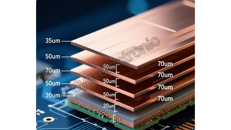
Why Is Copper Thickness Something You Should Set Before Trace Width?
As everyone should know, trace width can be adjusted later in the board layout, but copper thickness is a fabrication process parameter — once it’s written into the stackup specification, it’s basically locked. Changing copper thickness often means redoing the stackup, recalculating impedance, and may even require switching processes.
More critically: copper thickness and trace width are not the same thing. For the same 10 mil trace, 1 oz and 2 oz can pass nearly double the current, and the impedance changes along with it. Only by setting copper thickness first can trace width and impedance be discussed with any accuracy.
Worth noting: for many of those “board runs hot” or “impedance won’t calculate right” pitfalls, the root cause isn’t trace width — it’s that copper thickness wasn’t set correctly from the very beginning.
What Is Copper Thickness: What Does “oz” Actually Mean?
“oz” is not a unit of thickness, but the weight of deposited copper per square foot. 1 oz copper ≈ 35 µm (about 1.37 mil) thick; 2 oz ≈ 70 µm, and so on. Common specifications include 0.5 / 1 / 2 / 3 / 4 oz and above.
Remember one thing: the “1 oz” you see refers to the average thickness converted from the deposited copper weight, not the physical tolerance you measure. The copper thickness a PCB factory talks about usually means the finished copper thickness (including plating).
Current Carrying: How Does Copper Thickness Affect Temperature Rise?
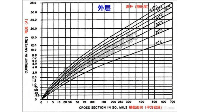
Current carrying depends on the conductor’s cross-sectional area = trace width × copper thickness. The thicker the copper, the larger the cross-section, and the smaller the temperature rise under the same current.
The current standard for judgment is IPC-2152 (the conductor current-carrying–temperature-rise standard, which has replaced the earlier IPC-2221 internal chart). What it gives is a curve of “how much current a given cross-section can carry under an allowed temperature rise,” and copper thickness is a direct input.
For high-current scenarios like power boards and motor drives, bumping from 1 oz to 2 oz often saves more area than simply widening the traces.
Impedance: The Hidden Effect of Copper Thickness on Controlled Impedance
When doing high-speed or RF, everyone stares at the dielectric constant and trace width to calculate impedance, yet easily overlooks copper thickness. In reality, copper thickness goes directly into the impedance formula: with the same trace width and spacing, the thicker the copper, the lower the characteristic impedance.
This means: if you calculate the impedance based on 1 oz but the board is built with 2 oz, the measured impedance will run low and may fall outside the tolerance band. For impedance-sensitive designs, copper thickness must be pinned down in the stackup spec just like trace width, and the finished copper thickness must be verified with the board house. See our guide on controlled impedance.
Heat Dissipation: How Does Thick Copper Carry Heat Away?
Copper itself is an excellent thermal conductor. Thick copper can spread local heat laterally, then carry it through thermal vias to inner layers or back-side copper planes and heatsinks, significantly lowering hot-spot temperature rise.
This is why power modules and LED drivers commonly use 2 oz or even thicker copper — not to make the traces fatter, but to make the board “know how to dissipate heat.” For boards limited by heat dissipation, ask about copper thickness first, then about thermal-conductive materials. Our PCB thermal management guide goes deeper on this.
The Cost: Thick Copper Isn’t a Universal Solution
Thick copper comes with a cost; balancing it comes down to three points:
- Etching limit: The thicker the copper, the more pronounced the side etching, and the larger the minimum etchable trace width. Empirically, 1 oz can reach about 3–4 mil, 2 oz needs about 6–8 mil, and heavy copper (≥3 oz) needs to be even wider. In dense BGA breakout areas, thick copper will directly jam it.
- Cost and process: Thick copper needs heavier deposition/plating, more process steps, and usually longer lead times and higher unit prices; ≥3 oz mostly belongs to power-specific processes, and not every factory can do it stably.
- Interlayer limits: Adding copper on outer layers is relatively flexible, but inner-layer thick copper is constrained by prepreg (semicured sheet) resin filling and the lamination window — so you shouldn’t add it blindly.
Thick copper isn’t a “more expensive upgrade pack,” but a trade-off for high current / high heat dissipation. Forcing 2 oz where 1 oz should be used will only buy you wider traces, tighter layout, and higher cost. For extreme thermal loads, a metal-core PCB may be the better call.
A Copper-Thickness Selection Reference Table
| Your scenario | Recommended copper weight | Reason | Note |
| General digital / signal boards | 0.5–1 oz | Fine lines and dense pitch; balance of cost and manufacturability | For high-speed impedance, calculate by finished copper thickness |
| Power / high-current traces | 2 oz | More stable current carrying and temperature rise; saves area | Widen trace width in breakout areas |
| Power modules / LED drivers | 3 oz+ | Lateral heat spreading + high current | Mostly specialized process; confirm the fab’s capability first |
| Inner-layer planes / ground | 1 oz (can go up to 2 oz) | Return path and heat dissipation | Constrained by prepreg resin filling |
| HDI / fine-pitch BGA | 0.5–1 oz | Decided by the etching limit | Thick copper will jam the breakout |
Frequently Asked Questions
How do you actually choose between 1 oz and 2 oz? Look at current and heat dissipation, not at “habit.” For signal boards 1 oz is enough; for high current or tight heat dissipation, prioritize 2 oz. First use IPC-2152 to calculate the temperature rise, then decide — don’t just decide off the top of your head.
Does copper thickness affect impedance? Yes, and it’s often overlooked. With the same trace width, the thicker the copper, the lower the impedance. Impedance-sensitive designs must write copper thickness into the stackup spec and verify the finished copper thickness with the board house.
Do you have to go thick copper for high current? Not necessarily. Widening traces, opening copper pours, adding thermal vias, or even using a metal-core board can all share the load. Thick copper is one means, not the only solution; sometimes window-opening and adding solder or running traces in parallel is more cost-effective.
How thin a trace can thick copper still route? Roughly 1 oz ≈ 3–4 mil, 2 oz ≈ 6–8 mil, and heavy copper needs to be wider. The specifics depend on the fab’s process capability; dense-pitch BGA breakout areas need to be checked in advance.
Can inner and outer layer copper thickness differ? Yes. Outer layers are often thicker due to plating, while inner layers are constrained by lamination. The stackup spec can define them separately, but each layer must be confirmed for manufacturability with the board house.
Why These Points Matter
Copper thickness isn’t a number you fill in casually on the fabrication parameter sheet. It simultaneously determines whether your board can carry current, whether the impedance is accurate, and whether the heat can dissipate — and once set early, it’s extremely hard to change later. First align the three things — current carrying, impedance, heat dissipation — then talk about trace width and stackup. Don’t let “default 1 oz” bury a board that should have been stable.
Reference Sources
- IPC — IPC-2152 conductor current-carrying–temperature-rise standard (current; replaces the older IPC-2221 internal chart)
- Industry general — 1 oz copper ≈ 35 µm (1.37 mil); common copper weights 0.5 / 1 / 2 / 3 / 4+ oz; minimum etchable trace width increases with copper weight
- Stackup and impedance — copper thickness is an input to the characteristic-impedance formula and must be verified against finished copper thickness with the board house
 English
 Русский
 Français
 Deutsch
 日本語
 한국어
 Español
 Português
 العربية
 Türkçe
 Italiano
 Polski
 Dansk