
Miniaturization drives innovation across the modern electronics frontier. This trend challenges engineering teams to fundamentally rethink printed circuit board (PCB) manufacturing processes. Among the most complex technologies in this shift is 01005 component assembly. These miniature passive devices measure just 0.4 mm x 0.2 mm, making them the smallest standard surface-mount components currently in mass production. Despite their size constraints, 01005 packages play a pivotal role in designing highly compact devices like smartwatches, IoT sensors, and next-generation smartphones. However, handling and assembling these components introduces significant complexity. This guide explores the specific technical challenges of the assembly process and provides validated solutions for achieving consistent production yields.
The Fundamental Nature of 01005 Components
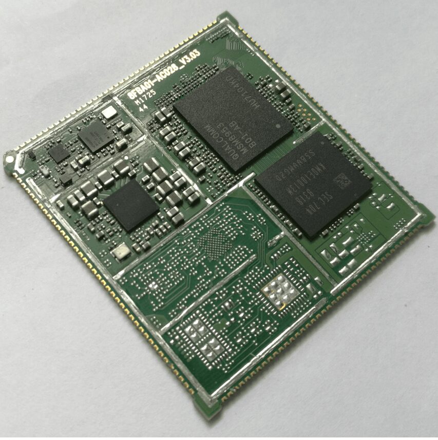
01005 components represent the cutting edge of miniaturized electronics. They function as essential elements in applications requiring high-density layouts. Their compact footprint allows designers to place them between pins on dense Ball Grid Arrays (BGAs), maximizing routing efficiency. Beyond high-tech applications, these miniature passive devices perform critical functions such as signal conditioning and power decoupling in constrained spaces. Successfully implementing them requires a deep understanding of their unique assembly characteristics rather than treating them as simple scale-downs of larger components.
Critical Challenges and Solutions in 01005 Assembly
Achieving reliable 01005 component assembly demands addressing five specific technical hurdles. Each challenge requires targeted process controls and equipment capabilities to prevent yield loss.
Challenge 1: Accuracy in Solder Paste Printing
Solder paste printing is typically the first and most critical process in Surface Mount Technology (SMT) assembly. The minute pad size of 01005 components requires an exceptionally high level of accuracy for correct solder deposition. Insufficient or excessive paste directly causes open circuits or solder bridges.
Technical Solutions:
- Advanced Stencil Technology: Employing high-quality stencils, specifically electroformed or laser-cut variants, is paramount. These stencils must feature well-defined apertures with optimized aspect ratios to maximize paste transfer efficiency. This reduces volume variability and ensures balanced solder distribution across all pads.
- Process Parameter Optimization: Engineers must refine printing parameters, including squeegee speed, pressure, and separation velocity. Integrating Automated Optical Inspection (AOI) for real-time paste verification is essential. Consistent application prevents defects arising from uneven deposits before placement even begins. For detailed specifications on stencil design, refer to the IPC-7525 Stencil Design Guidelines.
Business Value Highlight: Optimizing stencil aperture design and print parameters for 01005 pads can reduce post-reflow solder defects by up to 30%. This improvement directly lowers rework costs and accelerates time-to-market for high-density wearable and medical device prototypes.
Challenge 2: Component Placement Accuracy
Standard placement methods often prove inadequate for 01005 component assembly due to the extreme precision required. Minor misalignments that are tolerable for 0402 metric package or 0201 packages become catastrophic failures at this scale, potentially resulting in tombstoning or complete misplacement.
Technical Solutions:
- High-End Placement Equipment: Manufacturers must invest in advanced pick-and-place machines incorporating high-resolution vision systems. These systems improve placement accuracy to within ±0.025 mm or better. The equipment must be specifically calibrated to handle the fragility and dimensional tolerances of 01005 devices.
- Dynamic Process Adaptation: Utilizing machine learning algorithms enables adaptive placement correction. These systems analyze real-time feedback to adjust nozzle positioning dynamically, improving accuracy and minimizing human error during long production runs. For more on precision placement, explore our SMT Assembly capabilities.
Challenge 3: Controlled Reflow Soldering
Reflow soldering of 01005 devices presents unique thermal management challenges. The extremely low thermal mass of these components makes them highly sensitive to temperature gradients. Errors in profiling frequently cause tombstoning (where one end lifts off the pad) or bridging.
Technical Solutions:
- Precision Thermal Profiling: Engineers must create dedicated reflow profiles addressing the specific thermal properties of 01005 devices. Uniform heat distribution and controlled ramp rates are mandatory to prevent component migration when solder reaches its liquidus state. Soak zones may need adjustment compared to mixed-technology boards.
- Continuous Monitoring Systems: Implementing real-time thermal monitoring allows for adaptive control of the reflow oven. Sensors verify actual board temperatures rather than relying solely on setpoints, ensuring reliable solder joint formation across varying board densities. Industry best practices for thermal profiling are outlined in IPC/JEDEC J-STD-020.
Challenge 4: Successful Inspection and Quality Control
Inspecting 01005 packages pushes conventional Automated Optical Inspection (AOI) to its limits. Standard resolution cameras and lighting setups often fail to reliably distinguish valid joints from false calls, creating bottlenecks in quality assurance for ultra-fine pitch assembly.
Technical Solutions:
- Hybrid Inspection Methods: Integrating high-resolution AOI systems with targeted human verification for critical areas ensures accurate defect identification. This hybrid approach balances throughput with reliability for ultra-fine pitch features.
- Innovative Imaging Solutions: Advanced imaging technologies, including 3D SPI and multi-spectral lighting, help distinguish between genuine flaws and acceptable process variations. Enhancing defect detection effectiveness reduces escape rates without inflating false failure metrics. Adherence to IPC-A-610 Class 3 standards remains the benchmark for acceptance criteria in these inspections.
Challenge 5: Overcoming Rework and Repair Challenges
The combination of microscopic size and dense packing patterns makes reworking 01005 components exceptionally difficult. Traditional hot air or iron-based rework risks damaging adjacent components or delaminating the PCB substrate.
Technical Solutions:
- Proactive Defect Mitigation: Emphasizing strong first-pass yield through upfront Design for Manufacturing and Assembly (DFMA) and rigorous testing limits the need for rework entirely. Prevention is always superior to correction at this scale.
- Precision Rework Tools: When rework is unavoidable, utilize specialized micro-rework stations featuring precise heating control and optical guidance. These tools ensure the process remains localized and does not thermally stress neighboring components. Learn about our Prototype PCB Assembly services for DFMA-supported development cycles.
Partnering for Advanced Micro-SMT Success
Successfully integrating 01005 component assembly into PCB designs requires a holistic approach spanning design, technology, and continuous process improvement. Investments in advanced manufacturing equipment and optimization at every process step unlock the full potential of these miniature devices. Such efforts enable the production of more complex, compact, and highly advanced electronic products. At DYC Electronic, we support partners in tackling these difficulties through strict adherence to IPC standards and DFMA principles, ensuring first-class quality for high-density assemblies.
Frequently Asked Questions About 01005 Assembly
What makes 01005 component assembly different from 0201 or 0402 assembly?
01005 component assembly differs primarily in tolerance sensitivity and equipment requirements. While 0201 and 0402 metric package sizes allow some margin for error in paste printing and placement, 01005 devices demand sub-25-micron placement accuracy and specialized electroformed stencils. The thermal mass is so low that standard reflow profiles often cause tombstoning, requiring dedicated thermal characterization. Additionally, inspection requires higher resolution AOI systems capable of resolving features below 0.1 mm.
Can standard SMT lines handle 01005 component assembly without upgrades?
Most standard SMT lines cannot reliably handle 01005 component assembly without significant upgrades. Typical pick-and-place machines lack the vision system resolution and nozzle precision needed for 0.4 mm x 0.2 mm parts. Standard laser-cut stencils often exhibit insufficient aperture release for such small volumes. Facilities must typically upgrade to dedicated micro-placement modules, implement 3D solder paste inspection, and validate reflow ovens for ultra-low-mass components before attempting volume production.
What are the most common defects in 01005 component assembly and how are they prevented?
The most common defects in 01005 component assembly include tombstoning, solder bridging, and insufficient wetting. Tombstoning results from uneven heating or imbalanced pad geometry; prevention requires symmetric pad design and optimized soak zones. Bridging stems from excessive paste volume or misalignment; electroformed stencils with reduced aperture sizes mitigate this. Insufficient wetting often indicates oxidation or inadequate flux activity; using fresh Type 5 or Type 6 solder paste with high-activity flux chemistry addresses this issue. All three defects benefit from real-time SPI and AOI feedback loops.
Is rework feasible for 01005 components, or should boards be scrapped?
Rework on 01005 components is technically feasible but carries high risk and cost. Specialized micro-rework stations with optical magnification and localized heating are mandatory. Success rates depend heavily on operator skill and board density; densely packed areas near BGAs may be unreworkable without collateral damage. Many manufacturers adopt a “no-rework” policy for 01005 positions in high-volume production, focusing instead on achieving >99.5% first-pass yield through DFMA and process control. For prototype or low-volume builds, rework remains viable with proper tooling and trained technicians.
 한국어
한국어  English
  Русский
  Français
  Deutsch
  日本語
日本語  Español
  Português
  العربية
  Türkçe
  Italiano
  Polski
  Dansk
Dansk