
PCB Process Edge Design: SMT Rail Clearance Guide
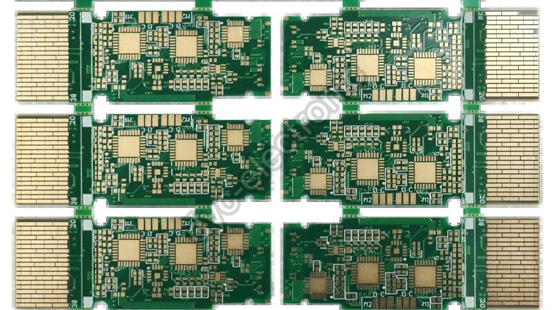
A 0402 capacitor sits 2 mm from the board edge. During SMT assembly, the conveyor rail clamps down and crushes it before reflow even starts. This happens more often than you’d think. In our builds, we see this failure when designers treat the PCB process edge design as an afterthought rather than a first-order constraint. The fix isn’t expensive, but catching it late costs real money in rework and delayed shipments. This guide walks through the exact margins, mark points, and separation methods that keep boards running smoothly on high-speed SMT lines. No theory dumps—just the parameters we verify during every DFM check. Why SMT Rail Clearance Defines Your PCB Process Edge […]
PCB Via Types: Cost, Design Rules & Selection Guide
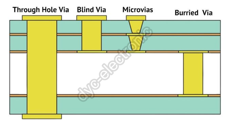
A 0.65mm pitch BGA sits on your layout. You need to escape 800 pins, but through-holes eat every routing channel they touch. Do you jump straight to PCB via types like microvias, or can a smarter stackup save the budget? We review over 200 via specifications weekly, and roughly 40% of boards specified with blind or buried vias could achieve identical routing with through-holes alone. Conversely, defaulting to through-holes when advanced structures are genuinely needed forces extra layers that cost more than the via upgrade itself. This guide gives you the real production cost multipliers, lead time impacts, and decision thresholds from our factory floor—updated as of 2026-09—to help you choose correctly […]
PCB vs PCBA: Key Differences for Electronics Buyers
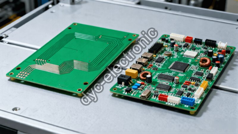
A purchasing manager once sent us a request for “500 PCBs” with a BOM attached, expecting fully functional units. We had to clarify that they actually needed PCB vs PCBA distinction understood before production started. This confusion happens more often than you’d think in electronics procurement. A Printed Circuit Board (PCB) is just the bare foundation, while a Printed Circuit Board Assembly (PCBA) is the finished, functional product with all components mounted. Mixing these terms up can lead to wrong quotes, delayed shipments, and failed prototypes. Let’s break down exactly what separates a bare board from a complete assembly, so your next RFQ hits the mark. What Is a PCB? The Bare […]
Common PCB Problems: 5 Defects Your Manufacturer Must Avoid
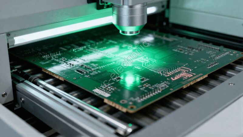
A single sharp corner on a copper trace can trap etchant during production. Weeks later, that trapped acid eats through the conductor from the inside out, causing an intermittent field failure that no functional test caught. This is just one of many common PCB problems that slip past inexperienced fabricators. In our builds, we have learned that preventing these defects requires specific validation checks at both the design and manufacturing stages, not just hope. Below, we break down five frequent issues and the exact countermeasures your contract manufacturer should be applying to protect your yield and reputation. Acid Traps: The Silent Etching Threat Acid traps form when etching solution pools in small […]
PCB Gerber Files: Formats & Manufacturing Use
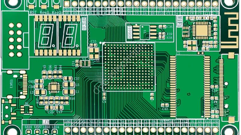
A missing aperture definition in your PCB Gerber files can halt a production line for days. We have seen entire batches of bare boards scrapped because the solder mask layer did not align with the copper pads, all due to a corrupted vector coordinate in the output zip. These files are not just digital paperwork; they are the direct machine instructions that translate your CAD design into physical hardware. Understanding what these files actually contain prevents expensive re-spins. Below, we break down the formats, generation process, and documentation standards that keep manufacturing running smoothly. What Are PCB Gerber Files Exactly? Originally developed by Gerber Scientific (founded by Joseph Gerber), this format became […]
Conformal Coating Exclusion Zones: 5 Parts to Mask
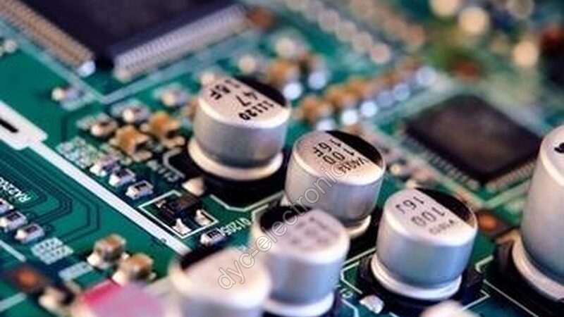
A fresh batch of industrial controller boards just failed field testing. The root cause? Conformal coating seeped into connector contacts during processing. This scenario repeats constantly in conformal coating exclusion zones management. Many engineers assume full-board coverage equals better protection. Actually, unmasked functional areas create invisible failure points that surface months after shipment. Understanding which components demand strict masking prevents costly rework and warranty claims. Connectors: Top Priority for Conformal Coating Exclusion Zones Connectors sit at the top of the conformal coating exclusion zones list because they depend entirely on metal-to-metal contact. Contact resistance typically measures only tens of milliohms when clean. Coating residue inside pin holes or mating surfaces creates an insulating film […]
PCB Thermal Management: Vias and Copper Pours That Work
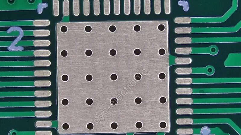
A MOSFET on a 5 W buck converter runs fine on the bench. Bolt it into a sealed enclosure, however, and the same part climbs past 110 °C within minutes. PCB thermal management is what separates a board that survives field use from one that cooks its own solder joints. Actually, heat is not a side effect you fix later. It is a layout decision you make on layer one. Why Your Board Overheats: The Heat Spreading Trap Heat in a PCB follows one unglamorous equation: ΔT = P × R_th. Power dissipated times thermal resistance equals the temperature rise above ambient. Specifically, a 1 oz copper plane on FR-4 […]
Bare PCB Quality Control: A Practical Guide to Testing and Reliability
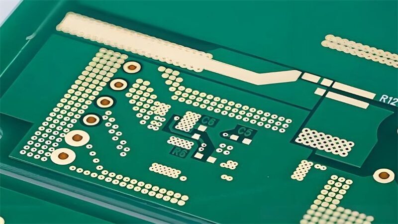
An unpopulated substrate equipped with copper traces, vias, pads, and dielectric layers serves as the fundamental carrier for nearly all electronic equipment. From consumer gadgets to high-performance aerospace systems, medical instruments, and industrial control devices, the bare PCB quality control process determines the final product’s success. Fabrication involves high-precision procedures like lamination, drilling, plating, imaging, etching, solder mask coating, and surface finishing. Each step introduces risks of defects such as broken traces, hidden shorts, uneven plating, or interlayer delamination. If defective boards reach assembly, they cause signal disorders, hardware failures, and safety hazards. Therefore, comprehensive testing is crucial to ensure performance, yield rates, and long-term reliability. Full-Process Bare PCB Quality Control Workflow […]
 日本語
日本語  English
  Русский
  Français
  Deutsch
  한국어
한국어  Español
  Português
  العربية
  Türkçe
  Italiano
  Polski
  Dansk
Dansk