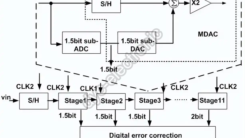
A temperature sensor reads 25.3 °C on your prototype but drifts to 26.1 °C after two hours of runtime. The MCU datasheet promises a 12-bit ADC, yet your measurements look noisy and inconsistent. This scenario frustrates many engineers during validation. Before blaming the sensor or rewriting firmware, you must verify whether the MCU built-in ADC vs dedicated ADC choice actually matches your signal chain requirements. Most physical signals in industrial and consumer electronics are analog. Temperature, pressure, audio, current, and displacement all vary continuously. Your digital processor needs an A-D converter to translate these real-world voltages into discrete codes. System designers generally face two paths: integrate the conversion inside the microcontroller or […]
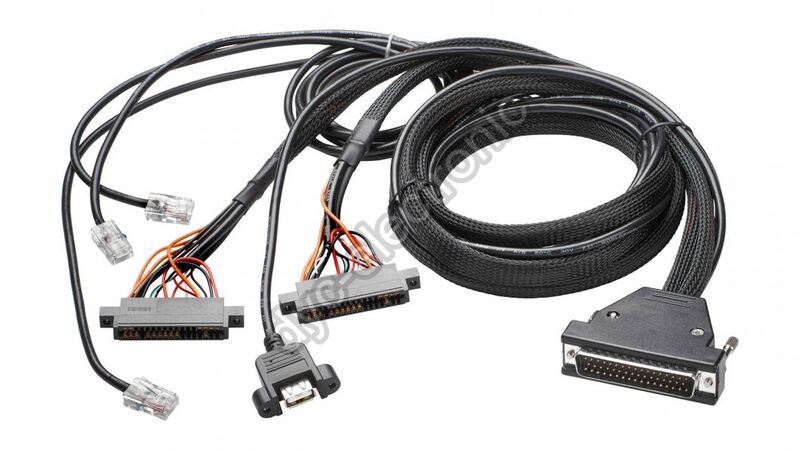
Choosing the right wire harness vs cable assembly starts before you request a quote. In casual conversation, engineers often swap these terms. On a purchase order, however, that ambiguity costs money. Mislabeling your interconnect can trigger a wrong quote or a product that fails in the field. Actually, these two constructs have genuinely different design requirements, manufacturing processes, and performance characteristics. This article defines each type clearly, explains the structural differences, and gives practical guidance on selecting the correct solution for your next build. What Is a Cable Assembly? A cable assembly is an organized grouping of one or more insulated conductors terminated at both ends with connectors or contacts. The defining […]
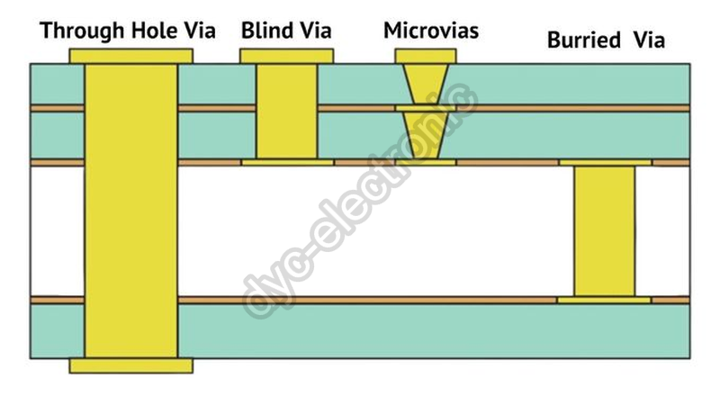
A 0.65mm pitch BGA sits on your layout. You need to escape 800 pins, but through-holes eat every routing channel they touch. Do you jump straight to PCB via types like microvias, or can a smarter stackup save the budget? We review over 200 via specifications weekly, and roughly 40% of boards specified with blind or buried vias could achieve identical routing with through-holes alone. Conversely, defaulting to through-holes when advanced structures are genuinely needed forces extra layers that cost more than the via upgrade itself. This guide gives you the real production cost multipliers, lead time impacts, and decision thresholds from our factory floor—updated as of 2026-09—to help you choose correctly […]
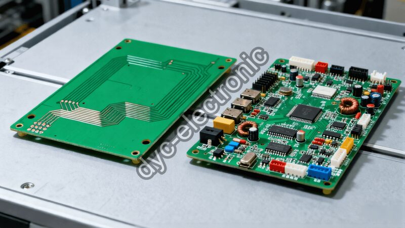
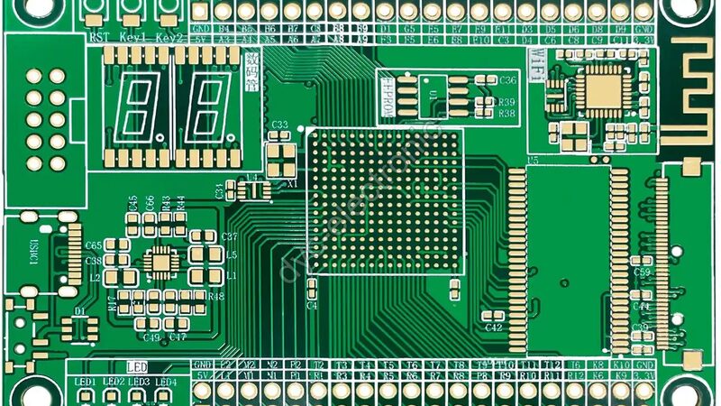
A purchasing manager once sent us a request for “500 PCBs” with a BOM attached, expecting fully functional units. We had to clarify that they actually needed PCB vs PCBA distinction understood before production started. This confusion happens more often than you’d think in electronics procurement. A Printed Circuit Board (PCB) is just the bare foundation, while a Printed Circuit Board Assembly (PCBA) is the finished, functional product with all components mounted. Mixing these terms up can lead to wrong quotes, delayed shipments, and failed prototypes. Let’s break down exactly what separates a bare board from a complete assembly, so your next RFQ hits the mark. What Is a PCB? The Bare […]
A single sharp corner on a copper trace can trap etchant during production. Weeks later, that trapped acid eats through the conductor from the inside out, causing an intermittent field failure that no functional test caught. This is just one of many common PCB problems that slip past inexperienced fabricators. In our builds, we have learned that preventing these defects requires specific validation checks at both the design and manufacturing stages, not just hope. Below, we break down five frequent issues and the exact countermeasures your contract manufacturer should be applying to protect your yield and reputation. Acid Traps: The Silent Etching Threat Acid traps form when etching solution pools in small […]
A missing aperture definition in your PCB Gerber files can halt a production line for days. We have seen entire batches of bare boards scrapped because the solder mask layer did not align with the copper pads, all due to a corrupted vector coordinate in the output zip. These files are not just digital paperwork; they are the direct machine instructions that translate your CAD design into physical hardware. Understanding what these files actually contain prevents expensive re-spins. Below, we break down the formats, generation process, and documentation standards that keep manufacturing running smoothly. What Are PCB Gerber Files Exactly? Originally developed by Gerber Scientific (founded by Joseph Gerber), this format became […]
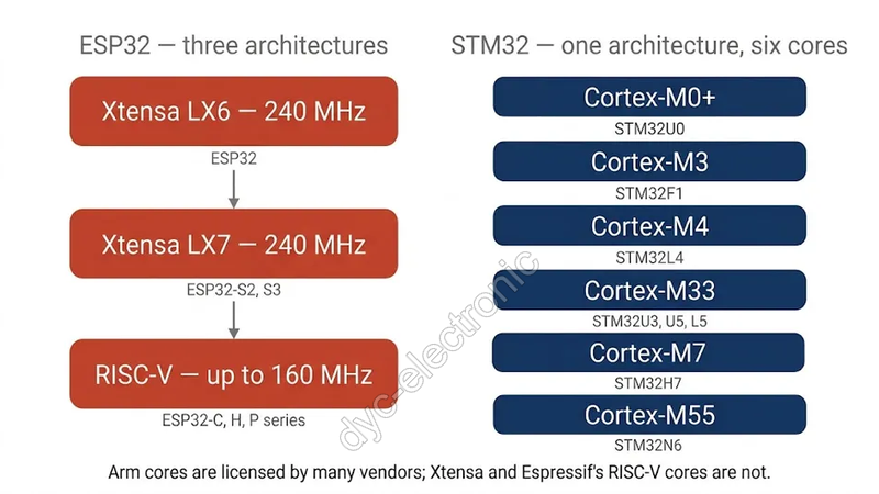
A 470 µF capacitor sits on the bottom side of a dual-layer board. Halfway through the second reflow pass, gravity wins and the part drops onto the conveyor belt. That is not an STM32 or ESP32 problem, but it illustrates how a single component choice cascades into PCBA assembly yield, test fixture design, and field reliability. When engineers ask us about STM32 vs ESP32, they are rarely asking which chip has more CoreMark points. They are asking which one keeps their product shippable, certifiable, and orderable for the next decade. In our builds, we have seen both platforms succeed and fail for reasons that never appear in a datasheet summary table. […]
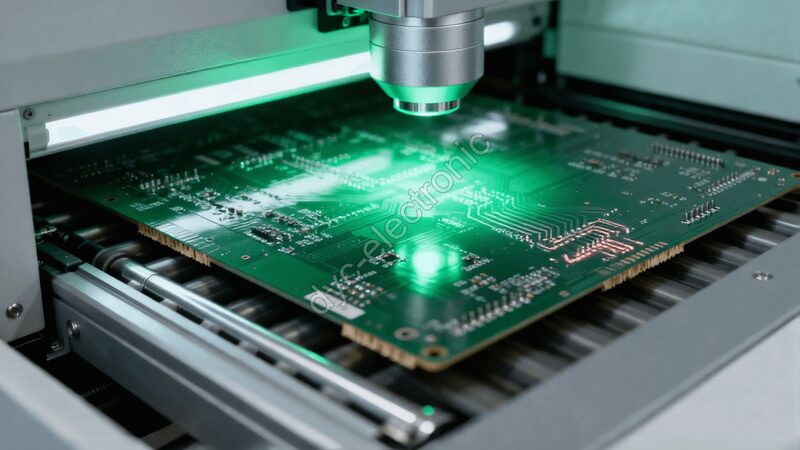
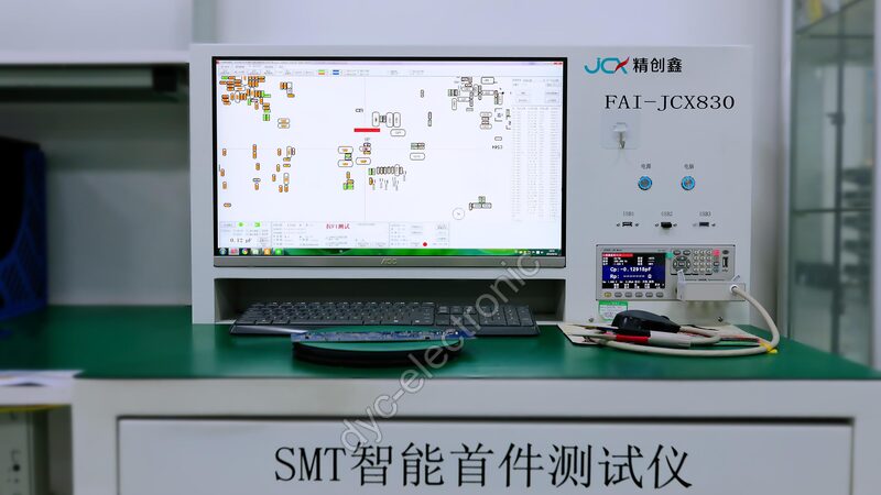
A single misaligned 0402 capacitor on the first board off the line can silently kill an entire production run. We have seen it happen: the reel was swapped during setup, nobody caught the polarity mark shift, and 500 units went through reflow before anyone noticed. That is exactly why first article inspection SMT exists as a mandatory checkpoint. It is not just paperwork; it is the only reliable gate between a correct setup and a costly batch failure. In our builds, we treat this step as non-negotiable, because catching one bad board now saves scrapping five hundred later. Why First Article Inspection SMT Matters on the Line Actually, FAI serves as your […]

 日本語
日本語  English
  Русский
  Français
  Deutsch
  한국어
한국어  Español
  Português
  العربية
  Türkçe
  Italiano
  Polski
  Dansk
Dansk