
The layout of the power section is far more than just connecting the chip and running the caps over. How close the input and output capacitors sit to the pins, how the ground return runs, how much copper you leave for the switch node, which side you take the feedback sample from — these details together decide the board’s ripple level, heat situation, and EMC performance. Below, the layout points of LDO and DC-DC are broken out separately, for engineers to refer to during the actual board drawing after the topology is settled at selection time.
1. The Fundamental Difference Between LDO and DC-DC
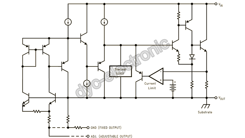
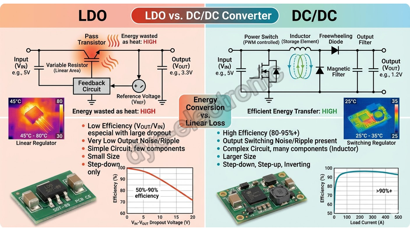
An LDO is a linear device; it steps down voltage by linear division through a pass transistor, with no switching action, so noise is very low, but efficiency is also capped by the voltage drop. A DC-DC (taking a typical buck step-down as the example) is a switching device; it transforms voltage by high-speed switching together with inductor energy storage, so efficiency is higher, but it brings switching ripple and EMI, and is quite sensitive to layout.
On selection: when the drop is small, current is modest, and noise sensitivity is high, LDO is often the better fit; when the drop is large, efficiency is required, current is larger, or battery power is used, DC-DC is often the better fit. The two have completely different concerns at the board-layout level, explained separately below. The parameters and experience values below are for reference only; actual values should follow the device datasheet and specific application conditions.
2. LDO Input and Output Capacitor Placement
An LDO’s periphery is usually simple (VIN, VOUT, GND, plus enable and feedback pins), but the placement of the input and output capacitors can’t be sloppy. These two capacitors handle regulation and ripple suppression; the farther from the pins, the larger the parasitic inductance, the more the regulation bandwidth tends to drop, and the easier it is to oscillate.
Ceramic capacitors are usually preferred. Compared to capacitance value, placement often matters more — in space-constrained cases, using a smaller value placed close to the pin is generally preferable to using a larger value placed far away.
3. LDO Ground Return Path
The GND pin’s current return path should go back to the system ground as directly as possible, avoiding detours. Reasonable large-area copper and appropriately more ground vias can provide a low-resistance return path for the current. The length and width of the ground loop should be judged against the board layer structure, device package, and actual current demand — there is no fixed value that fits all cases.
4. LDO Thermal Handling
An LDO’s own power dissipation can be approximated as Pd = (VIN − VOUT) × IOUT + VIN × IGND. When the drop is large and current is large, this portion of power basically turns into heat. Relying only on the device’s own small-area dissipation is often not enough; you can lead the heat out through copper pour and thermal vias.
Modern LDOs’ dropout commonly falls in the 100–300mV range, and ultra-low-dropout devices can get below 100mV (specific per datasheet). The smaller the drop, the smaller the heat generation under the same conditions, usually.
5. DC-DC Input Loop
For a buck topology, the core of the layout can be summed up in one sentence: keep the area of the high-frequency, high-current loop as small as possible. The input loop refers to the segment from the input capacitor to the high-side switch, then to the low-side switch and ground; this is where the steepest di/dt flows. The input capacitor should be placed as close as possible to the VIN and GND pins (commonly within a few millimeters, depending on switching frequency and device requirements). When the loop area is too large, both EMI and input ripple grow with it.
6. DC-DC Switch Node
The switch node (the point where the high-side and low-side switches connect to the inductor) is a high-frequency, large-swing AC node; its dv/dt can reach tens of V/ns, and it’s usually the primary noise source on a DC-DC board. The copper area of this node should be as small as possible, the trace as short as possible, and kept away from sensitive regions like feedback, analog, and RF. The control of area or trace length should be weighed against the device manual’s recommendations and the distribution of sensitive circuits across the whole board.
7. DC-DC Output Loop and Ground Plane
The output loop refers to the segment from inductor, output capacitor to ground; its di/dt is relatively mild, but the output capacitor should also be placed close. The ground is generally recommended to use a complete ground plane, letting the power ground return be direct and as short as possible. How power ground and sensitive analog ground connect should follow the device manual’s guidance on PGND and AGND, and should not be arbitrarily set to single-point ground or star structure on your own.
8. DC-DC Inductor and Heat-Dissipating Devices
The inductor should use a shielded type — neither pressed against sensitive analog or RF devices (to avoid leakage magnetic coupling), nor placed too far from the IC. The IC, the inductor, and the freewheeling diode in a non-synchronous architecture are all heat-generating devices; enough copper pour should be reserved for them to help dissipation.
A buck converter’s efficiency can usually reach about 85–95%, and the switching frequency commonly falls in the 100kHz to 2MHz range (both per datasheet). The gain in efficiency and size comes at the cost of layout effort that cannot be skipped.
9. Feedback Network Placement
A DC-DC’s feedback (FB) is a low-voltage signal sampled from the output, most afraid of having noise coupled in from the switch node. Placement usually pays attention to the following:
- Feedback resistor close to the FB pin, don’t pull it far.
- Feedback trace away from the switch node and inductor; when conditions allow, run it on a quieter layer and use ground as protection.
- Take the sample point at the output capacitor or load end (Kelvin sensing), avoid taking it far from the capacitor, otherwise line loss gets counted into the feedback and causes the regulation point to drift.
- The divider network leans toward the output side, not the switching side.
10. LDO vs DC-DC Layout Points Comparison
The table below summarizes the points above for quick comparison. The values and descriptions in the table are general references; for actual application please confirm against the datasheet and specific working conditions.
| Dimension | LDO | DC-DC (buck) |
| Core device | Linear pass transistor | Switching transistor + inductor + diode |
| Efficiency | Lower (about VOUT/VIN, worse with large drop) | Higher (commonly 85–95%) |
| Noise / ripple | Extremely low, no switching ripple | Has switching ripple and EMI, layout-sensitive |
| Layout key | Input/output caps close, ground loop short, heat handled | Input loop small, switch node small and away from sensitive, feedback isolated, ground plane complete |
| Easy-to-fail points | Caps too far cause oscillation; large drop causes heat | Switch node too large or near sensitive causes radiation exceed; feedback coupled causes regulation drift |
| Applicable scene | Low drop, low noise, small current | Large drop, high efficiency, large current, battery powered |
11. Common Misconceptions
A few cognitive biases worth noting:
- Treating power as “just connect it”: in reality an LDO can oscillate, a DC-DC can exceed radiation limits; the layout itself decides success or failure.
- Thinking an LDO capacitor is better placed farther for convenience: the opposite — closer is usually steadier, placement matters more than capacitance.
- Thinking a DC-DC switch node can run a bit longer with no harm: that’s the biggest noise source; a bit longer means easier radiation and coupling.
- Feedback trace routed casually: once coupled by the switch node, you get regulation drift and noise into the loop.
- Using an LDO to carry large drop and large current: the power basically all turns to heat, efficiency very low; such cases should usually consider DC-DC.
12. Selection and Cascading
When low noise is needed (RF, ADC reference, audio, sensors, etc.), drop is small, current is modest → lean LDO; when high efficiency is needed (battery power, large drop, large current, heat-limited) → lean DC-DC.
The compromise is to first let DC-DC drop the voltage substantially (efficiency first), then follow with an LDO to further suppress ripple and noise, specifically to power sensitive analog or RF circuits. This DC-DC-plus-LDO cascade structure is fairly common in scenes like automotive infotainment, industrial acquisition, and aviation avionics. For certified projects with power-integrity and EMI requirements (such as automotive IATF 16949, aviation AS9100, industrial ISO 9001), this layout effort should not be omitted.
Conclusion
Power is the foundation of the whole board. An LDO looks simple, but with caps and ground not placed right it can oscillate; a DC-DC looks efficient, but with switch node and feedback not laid out right it can exceed radiation and drift regulation. The two can’t use the same drawing playbook — an LDO pursues “close and quiet,” a DC-DC pursues “small loop and noise isolation.” These details, if not taken seriously at the prototype stage, will cost far more to re-spin the board later when EMC fails before mass production and the whole unit develops strange noises, than the few extra vias and moving a capacitor a few millimeters now. For specific values and practices, always follow the device datasheet and actual manufacturing and assembly capability.
 العربية
 English
 Русский
 Français
 Deutsch
 日本語
 한국어
 Español
 Português
 Türkçe
 Italiano
 Polski
 Dansk