
A single sharp corner on a copper trace can trap etchant during production. Weeks later, that trapped acid eats through the conductor from the inside out, causing an intermittent field failure that no functional test caught. This is just one of many common PCB problems that slip past inexperienced fabricators. In our builds, we have learned that preventing these defects requires specific validation checks at both the design and manufacturing stages, not just hope. Below, we break down five frequent issues and the exact countermeasures your contract manufacturer should be applying to protect your yield and reputation.
Acid Traps: The Silent Etching Threat
Acid traps form when etching solution pools in small geometric pockets during the copper removal step. These trapped chemicals continue corroding long after the rinse cycle, creating faulty traces or open circuits. Trace angles below 90 degrees are the primary culprit, as they create acute corners where fluid dynamics prevent proper washout.
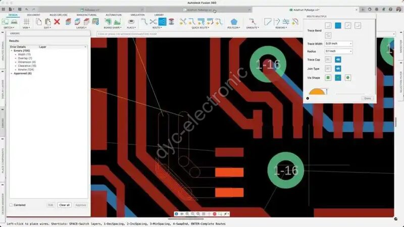
To control this, manufacturers must run automated DFM validation specifically targeting acute angles. We check for sharp corners that could act as potential traps before panelization begins. Additionally, verifying teardrop presence at via breakout points prevents wicking and mechanical stress concentration. If your fab house skips this geometric review, acid traps will eventually reach your field units.

BGA Spacing and Via Placement Errors
During BGA assembly, insufficient clearance around pads leads to solder bridging or insufficient wetting. Pads located directly under the die are especially vulnerable because reflow heat distribution becomes uneven. Improper via positioning relative to the ball grid array further compounds these PCB manufacturing defects.
Validation here demands precision. Ensure enough clearance space exists around every BGA pad according to IPC-7351B land pattern standards. Through-hole vias need positioning at the center of four adjacent BGA pads whenever possible to maintain uniform thermal mass. Actually, skipping this check is how you get hidden voids that fail only after thermal cycling in the field.
Tombstone Effect During Reflow
The tombstone effect occurs when a passive component lifts vertically at one end during reflow, resembling a gravestone. Uneven wetting forces cause this; if one pad reaches liquidus temperature faster than the other, surface tension pulls the part upright. This remains one of the most visible common PCB problems in high-volume SMT lines.
Prevention starts with balanced copper geometry. Ensuring connected copper at both pads stays within allowed limits equalizes heat absorption. In practice, we also verify that trace widths feeding each pad are symmetrical. Watch the pad size too—oversized pads on one side guarantee uneven heating regardless of stencil aperture adjustments.
Engineer’s Note: Tombstoning isn’t always a paste issue. Before blaming the solder paste supplier, measure the copper area ratio between both pads. A >15% imbalance almost always points to layout asymmetry, not chemistry.
Missing Test Points Kill Diagnostics
Test points provide electrical access for in-circuit testing and debugging. Without adequate coverage, diagnosing failures at the PCBA assembly validation stage becomes guesswork. You cannot fix what you cannot probe, and missing test points force technicians into destructive troubleshooting methods.
This problem originates entirely at the design stage. Ensure test points are incorporated for all critical nets before releasing Gerbers. Specifically, place them on one side of the board when possible to simplify fixture design. Furthermore, maintain minimum spacing per your CM’s test probe specifications. Skipping this step saves minutes during layout but costs days during prototype debug.
Silkscreen and Visual Feature Mistakes
Overlay layers carry reference names, component outlines, and polarity marks essential for assembly and repair. Errors here include placing reference designators over pads, hiding them under components, or misaligning pin-1 markers for complex ICs. Such mistakes slow manual inspection and increase rework time significantly.
Validation requires a dedicated silkscreen audit. Ensure reference names are accurate and sequenced correctly across the entire board. Check for first pin marks on all polarized and multi-pin devices. Moreover, confirm that no text overlaps with exposed copper or solder mask openings. That said, even perfect silkscreen won’t save a board if the underlying etching process control is weak.
Three Root Causes Behind Manufacturing Defects
Beyond individual defect types, common PCB problems typically originate from three systemic areas. Understanding these helps you evaluate whether a manufacturer truly has preventive controls or merely reacts to failures.
Material Selection Mismatches
Certain laminates suit specific circuit requirements; choosing wrong base materials severely impacts signal integrity and thermal performance. Operating environment dictates material choice as much as electrical specs do. For instance, high-Tg FR-4 may survive lead-free reflow but still delaminate in humid outdoor enclosures. Always validate Tg, CTE, and moisture absorption against your actual deployment conditions, not just datasheet typicals.
Component Lead Time Blind Spots
Selecting components without checking availability creates hidden schedule risks. Long lead times affect time-to-market and competitiveness more than any fabrication delay. In our experience, designers often lock in obsolete or allocation-prone parts before consulting procurement. Consequently, production stalls while sourcing alternatives. Engage your CM early to flag supply chain risks during BOM review, not after tooling is ordered.
Design for Manufacturability Gaps
Design-stage oversights include missing fiducials for fine-pitch parts, insufficient clearance, and components placed too close together. Robust DFM practices catch these before copper is etched. Choosing the right contract manufacturer matters critically here—they should proactively identify such issues rather than waiting for your explicit request. Refer to our PCB fabrication process controls page for details on how systematic DFM reviews prevent downstream failures.
Prevention Protocols Beyond Basic Inspection
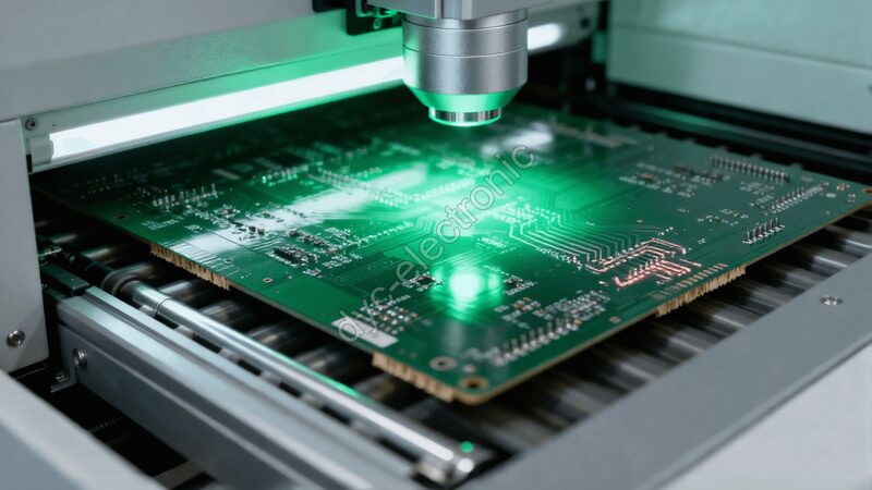
Avoiding errors requires layered verification. Keep PCB panels clean throughout processing to eliminate contamination-induced solder defects. Ensure visual inspection and electrical testing cover both sides of double-sided assemblies. Additionally, undertake micro-sectioning analysis periodically to validate internal layer registration and plating quality. Environmental factors like humidity storage and ESD handling also demand documented controls. Only manufacturers with robust expertise manage these nuances consistently.
For deeper insights into assembly-stage quality gates, explore our PCBA assembly validation resources covering AOI, X-ray, and functional test integration.
Procurement Tip: Ask potential suppliers for their micro-section report frequency and acceptance criteria. Manufacturers who treat cross-sectional analysis as optional are gambling with your internal layer integrity.
Frequently Asked Questions About PCB Failures
What causes a PCB to fail in a boiler?
Boiler environments combine thermal cycling, vibration, and moisture exposure. Damaged or weak solder joints crack under repeated expansion cycles. Fractures propagate through copper traces or laminate interfaces over time. Leaking boilers introduce water directly onto energized boards, accelerating electrochemical migration. Preventive measures include conformal coating, strain-relieved connectors, and potting for critical modules.
What temperature will damage a PCB?
High-temperature PCBs using polyimide or specialized laminates withstand continuous operation up to 150°C. However, standard FR-4 boards manufactured from materials with lower heat resistance operate safely only below 130°C. Exceeding Tg causes irreversible dimensional changes and delamination. Always match laminate grade to your maximum ambient plus self-heating margin, not just peak reflow tolerance.
Can water damage a PCB?
Yes, water damage ranks among the top causes of catastrophic PCB failure. Boiler systems contain numerous electronic controls vulnerable to leaks from heat exchangers or pumps. Even brief exposure initiates corrosion and dendritic growth that progresses silently. Conformal coatings rated IP67 or higher provide essential protection, but only if applied without voids at connector interfaces and component edges.
Secure Your Yield With Proactive DFM
Understanding common PCB problems is the first step; enforcing prevention protocols at your chosen factory is what actually protects your product. Don’t wait for field returns to discover your manufacturer skipped acid trap checks or BGA clearance validation. Request a free DFM review today and get a detailed risk assessment before your next build starts. Fill out the inquiry form below or email us directly for a competitive quote with full transparency on inspection standards.
 العربية
  English
  Русский
  Français
  Deutsch
  日本語
日本語  한국어
한국어  Español
  Português
  Türkçe
  Italiano
  Polski
  Dansk
Dansk