
Precision defines success in electronics manufacturing. Even minor process imbalances can trigger significant defects during production. PCB tombstoning remains one of the most frequent issues in surface mount technology (SMT). This defect occurs when a component lifts on one end during solder reflow and stands vertically on the board.
Engineers often call this the tombstone effect in PCB assembly. It typically affects small passive components like resistors and MLCC capacitors. Consequently, this issue directly impacts product reliability, yield rates, and overall production efficiency. Understanding the root causes and prevention methods is essential for achieving high-quality SMT PCBA services.
What Is PCB Tombstoning?
PCB tombstoning is a specific manufacturing defect occurring during reflow soldering. A small two-terminal surface-mount component lifts on one end. It then stands vertically on a single solder pad. This position creates an open circuit and renders the component non-functional.
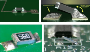
Why PCB Tombstoning Happens
Uneven surface tension forces primarily cause this issue during reflow. One end of the component wets before the other, creating an imbalance. Several key factors drive this phenomenon:
- Thermal Imbalance: One solder pad reaches melting temperature first. This creates an uneven pulling force that lifts the component upright on the first-melting side.
- Layout and Design Issues: Unequal pad sizes create thermal mass differences. Connecting one pad to a large copper area, such as a ground plane, also causes imbalance because that side heats or cools at a different rate.
- Manufacturing Variations: Inconsistent solder paste volume contributes to the problem. Uneven paste printing or slight misalignment during placement further increases risk during reflow.
How PCB Tombstoning Occurs in SMT Assembly
This defect manifests specifically during the reflow soldering stage. The failure sequence follows a predictable pattern in PCBA manufacturing:
- Solder paste prints onto PCB pads.
- Pick-and-place machines position components.
- The PCB enters the reflow oven.
- One pad heats faster than the opposite pad.
- Uneven solder wetting creates a force imbalance.
- The component lifts and stands upright.
Small MLCC components face the highest risk during this process flow.
Primary Causes of PCB Tombstoning
Multiple design and process-related factors contribute to the tombstone defect in PCB assembly. The table below outlines these critical variables:
| Cause | Описание | Impact |
|---|---|---|
| Uneven Heating | One pad reaches melting temperature earlier | Creates imbalance in solder wetting |
| Asymmetric Pad Design | Unequal pad size or shape | Results in uneven thermal mass |
| Solder Paste Issues | Incorrect volume or uneven printing | Causes poor wetting force balance |
| PCB Thermal Imbalance | Unequal copper distribution or routing | Makes one pad heat slower |
| Component Size | Small MLCCs or resistors | Increases sensitivity to surface tension |
| Reflow Profile Issues | Fast ramp or poor soak control | Leads to uneven solder melting |
| Contamination | Oxidation or moisture in paste/pads | Results in weak solder bonding |
Physical Mechanisms Behind the Tombstone Effect
Surface tension imbalance drives the physics of this defect during solder melting. Four main physical factors interact to lift the component:
- Surface tension force imbalance between pads.
- Thermal gradient existing between connection points.
- Vapor pressure generated during reflow.
- Component float caused by excess solder paste.
Impact of PCB Tombstoning on Production
The tombstone defect significantly affects both manufacturing quality and end-product performance. Key impacts include:
- Open circuits due to disconnected pads.
- Signal failure in finished electronic devices.
- Increased rework and repair costs.
- Lower production yield in SMT lines.
- Reduced long-term product reliability.
Therefore, addressing this issue early protects profit margins and brand reputation.
How to Prevent PCB Tombstoning
Prevention requires strict control over design, materials, and process parameters. Implement these best practices to mitigate risk:
Symmetrical Pad Design
Ensure both pads are identical in size and shape. Always follow IPC or manufacturer footprint standards to maintain balance.
Balanced Solder Paste Printing
Use accurate stencil designs to ensure consistency. Maintain equal paste volume on both pads to equalize wetting forces.
Optimized Reflow Profile
Apply a gradual temperature ramp-up to minimize thermal shock. Ensure uniform heat distribution across the PCB. Provide proper soak time for balanced melting.
PCB Layout Optimization
Avoid unequal copper distribution near component pads. Use thermal reliefs for connections to large planes. Maintain balanced trace routing to prevent heat sinking effects.
Accurate Component Placement
Ensure precise centering during the placement phase. Regularly calibrate pick-and-place machines to maintain accuracy.
Material and Paste Quality Control
Store solder paste properly to preserve its properties. Avoid oxidation and contamination at all costs. Use fresh and well-mixed paste for every production run.
Role of Design for Manufacturability (DFM)
Most tombstone defects in PCB assemblies can be prevented during the design stage. DFM practices identify risks before production begins. Key focus areas include:
- Correct footprint construction based on datasheets.
- Equal pad spacing and geometry verification.
- Balanced thermal mass design analysis.
- Proper routing symmetry checks.
- Standardized component library management.
Partnering with an experienced electronic components sourcing provider ensures your BOM aligns with manufacturable footprints. This proactive step reduces costly revisions later.
Why Choose DYC for Your PCB Manufacturing Partner
Selecting the right partner is essential for preventing defects like PCB tombstoning. DYC employs a manufacturing-driven design philosophy. We optimize every layout for real-world production to reduce the tombstone effect in PCB assembly. Our engineering team provides direct collaboration to resolve challenges quickly.
We offer a fast prototype-to-production workflow. Customers move efficiently from development to full-scale manufacturing without delays. Our expertise in high-speed PCB layout design maintains signal integrity alongside manufacturability. All projects follow strict IPC-compliant standards. Built-in DFM and DFT optimization minimizes production risks.
Furthermore, we support complex multilayer designs for high-density applications. Our capabilities in RF design strengthen performance in demanding systems. Quality is backed by ISO 9001:2015 certification for international quality management. DYC serves as a reliable engineering partner focused on reducing defects and delivering production-ready boards.
Contact us today to discuss your project requirements. Let us support you with high-quality manufacturing, DFM optimization, and fast turnaround solutions.
Frequently Asked Questions About PCB Tombstoning
1. Which PCB components are most prone to tombstoning?
Small passive components like MLCC capacitors, chip resistors, and inductors are most susceptible. Their light weight makes them highly sensitive to uneven surface tension during reflow soldering.
2. Can PCB tombstoning occur after the reflow process is completed?
No, tombstoning typically occurs only during the reflow soldering stage. Once solder fully cools and solidifies, the component position becomes fixed. However, inspectors usually detect the defect during post-reflow inspection.
3. Does PCB material affect the risk of tombstoning?
Yes, PCB material and copper distribution influence heat flow significantly. Uneven thermal conductivity across the board creates temperature differences between pads. This disparity increases the risk of tombstoning.
4. Can tombstoning be completely eliminated in SMT production?
Eliminating it 100% in all cases may not be possible. However, proper DFM practices, controlled reflow profiles, and optimized stencil design can significantly reduce occurrences. Continuous process monitoring further minimizes risk.
5. How is PCB tombstoning detected during manufacturing?
Automated Optical Inspection (AOI) systems usually identify it after reflow soldering. Manual inspection or electrical testing can also detect it. Electrical tests reveal the open circuit behavior caused by the lifted component.
 Русский
  English
  Français
  Deutsch
  日本語
日本語  한국어
한국어  Español
  Português
  العربية
  Türkçe
  Italiano
  Polski
  Dansk
Dansk