
Verifying circuit functionality during development is critical for any electronic product. PCB test points serve as essential access nodes that allow engineers to inject signals and monitor board performance. At DYC Electronic, we integrate these verification features early in the PCBA prototyping phase to prevent costly failures later. This guide covers every technical aspect of implementation to help you optimize your next design.

Understanding Verification Access Nodes
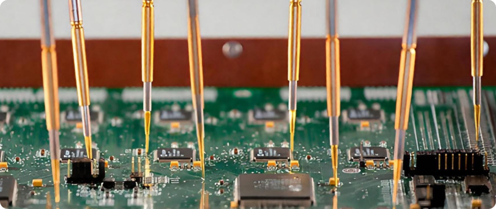
A PCB test point is typically a small wire loop or exposed metal pad. Engineers use it to inject test signals and monitor the board’s circuitry directly. Comparing the output against desired results enables optimal design adjustments. These points must reside on the outer layer of the board for probe accessibility. Furthermore, probe tips come in various shapes to accommodate different testing surfaces and contact requirements.
Categories of Circuit Board Testing
Understanding the specific category ensures you select the right verification method. They generally fall into two primary categories based on access method and automation level.
Manual Probe Access
This type provides an accessible point for handheld devices. Technicians use it primarily for surface-level testing. For instance, measuring current supply and ground values often requires this manual approach. It offers flexibility during initial debugging phases without needing complex fixtures.
Automated Verification Methods
Automated systems rely on dedicated PCB test points for high-volume verification. These include vias, through-hole pins, and metal landing pads. Automated testing itself divides into three distinct subtypes:
- Bare Board Testing: This occurs before component assembly. Its prime purpose is ensuring consistent electrical conductivity across the bare substrate.
- In-Circuit Testing (ICT): ICT verifies if all assembled components function flawlessly within the circuit. It checks individual part values and connections.
- Flying Probe Testing (FPT): FPT detects specific issues without custom fixtures. It identifies shorts, opens, resistance value deviations, and incorrect component orientation efficiently. For detailed technical standards on flying probe methodology, refer to the IPC-9252 specification.
Critical Signals Requiring Monitoring
Not every net needs verification access. However, specific signals benefit significantly from having dedicated PCB test points. Including them simplifies troubleshooting and validation. The following signals should always have designated test access:
- Power supply rails
- Ground connections
- Programming connections
- JTAG ports
- Serial communications busses
- Reset lines
- UARTs
- Programmable references
- Interrupt lines
Implementing Verification Features in Layout
Effective implementation requires proper setup. First, ensure the access node is an exposed metal spot on the outer layer. Probes must make solid physical contact for accurate readings. Designers can designate thru-hole pins and vias as valid locations.
Next, identify correct locations using your PCB design software. Most tools allow you to set parameters for automatic assignment. Once identified, export this data into a dedicated file. Modern design systems simplify generation significantly. Additionally, utilizing built-in verification features enhances overall quality and reduces manual errors. Always consult component datasheets, such as those found on Mouser Electronics, to verify pad compatibility before finalizing placement.
Benefits of Strategic Test Point Integration
Integrating PCB test points delivers tangible benefits throughout production. Their profile resembles surface mount components, making them versatile and easy to fit. More importantly, they identify issues during early design phases. This prevents costly errors from propagating to mass production stages.
Consequently, error detection becomes straightforward without compromising the core PCB design. For complex projects requiring turnkey PCBA services, these points streamline the entire validation workflow. They ultimately save both time and budget by catching defects when fixes are cheapest.
Essential Layout and Spacing Rules
Proper placement is just as important as inclusion. Adhering to established guidelines ensures manufacturing success and testing efficacy. Keep these five rules in mind during layout:
- Place all verification nodes on the same side of the board whenever possible.
- Maintain a minimum distance of 0.100 inches to ensure probe clearance.
- Distribute nodes uniformly across the board area.
- Keep tall components in designated areas so they do not block probe access.
- Account for manufacturing tolerances when accommodating probes.
Limiting excessive nodes also prevents accidental shorts and circuit damage. Following these standards guarantees reliable verification without introducing new risks.
Summary
Adding PCB test points facilitates easy error detection and generates significant savings in time and cost. While essential for verifying integrity, strict adherence to design guidelines remains mandatory. Proper implementation prevents future problems and protects your investment. DYC Electronic provides comprehensive PCB fabrication, assembly, and design services under one roof to support your testing needs. Contact our engineering team today for a free quote or consultation on your next project.
Frequently Asked Questions About PCB Test Points
1. How big should a PCB test point be?
Larger sizes work better because they make probe tip alignment easier. Ideally, a 0.050-inch PCB test point diameter works well for most standard applications. This size balances space efficiency with reliable mechanical contact.
2. How do you know if your PCB is shorted?
Several indicators reveal a short circuit. You might witness visual damage such as a cracked IC or blown capacitor. An acrid smell often accompanies thermal damage. Electrical testing via PCB test points confirms the exact location of the fault.
3. How do you choose a PCB test point location?
Follow specific guidelines when choosing locations. Place PCB test points on the same side of the board and distribute them evenly. Always maintain a minimum distance of 0.100 inches between adjacent points to prevent probe interference and ensure consistent access.
 Polski
  English
  Русский
  Français
  Deutsch
  日本語
日本語  한국어
한국어  Español
  Português
  العربية
  Türkçe
  Italiano
  Dansk
Dansk