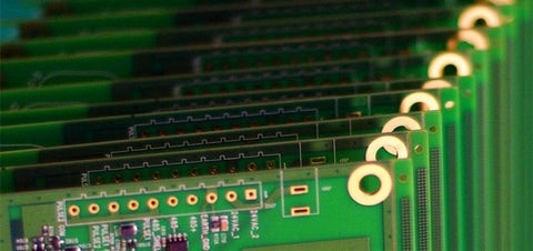
After the SMT patch proofing of the SMT small batch patch processing factory is completed, some follow-up processing procedures, such as testing, assembly, etc., are required. After all the electronic processing links are completed, it is delivered to the customer. It is relatively easy to be disturbed by various factors in the delivery and transportation process, such as bumps, collisions, friction, etc. So how should the PCBA factory transport it to ensure that the circuit boards processed by SMT are not damaged and reach the customers safely? The advantages of SMT chip processing: high assembly density, small size and light weight of electronic products, the volume and weight of chip […]
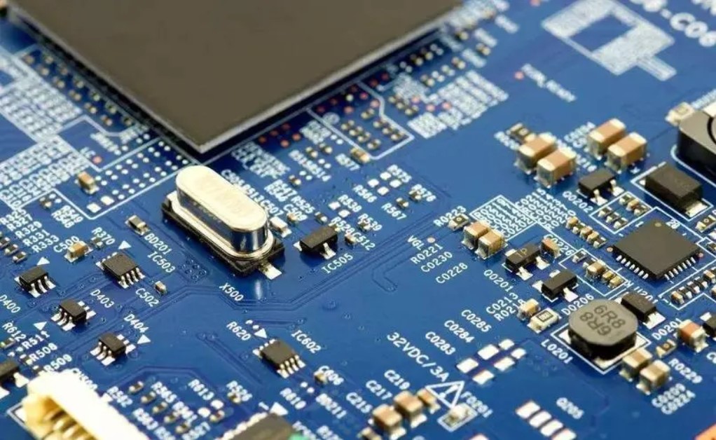
Every PCB assembly manufacturer must adhere to proper cleaning standards. Now the appearance of the circuit board cleanliness requirements are more and more strict, without affecting the work of the board, our DYC factory has been working hard to deliver a clean circuit board to each customer。 1.Comply with IPC-5704 All medical device development must meet a specific set of quality control standards. Ipc-5704 is a set of standards specifically addressing cleanliness requirements for the manufacture of unassembled printed circuit boards. A large part of this needs to go through the necessary steps to prevent and remove any kind of ionic contamination or other unwanted debris from the Integrated […]
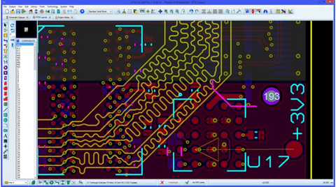
TWELVE BEST PCB DESIGNING SOFTWARE TOOLS In the market there is a large variety of PCB design software available. Some are proprietary, some are free to use online, and others are industrial grade PCB software. The following is a list of software EDA tools which PCB HERO Inc has compared for their performance. ALTIUM DESIGNER (PROTEL) This software, introduced in the late 1980s, is one of the best commercial PCB CAD design software available. Ranked highly among all other CAD software, there is a huge community support for the package providing a large library of footprints and other useful items. Many universities provide specific courses that teach use of PROTEL. […]
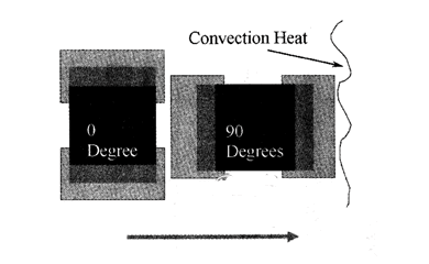
On the test board, the components are placed in two directions, 0 ° and 90 °. Determine whether component orientation (0 ° and 90 °) significantly affects the yield of assembly by analyzing paired samples. The 0 ° direction indicates that both ends of the component pass through the furnace simultaneously, while the 90 ° direction indicates that one end of the component passes through the furnace before the other end, as shown in Figure 1.Direction of components The hypothesis verified is: The virtual assumption is that z=0- there is no statistically significant difference in the number of assembly defects between the 0 ° and 90 ° directions. Furthermore, assuming that […]
According to the PCB design process, after the PCB layout was completed, a rigorous review process is required to determine whether the designed product meets the ESD or EMI requirements. Excluding schematic design, PCB design generally required to review both layout and wiring. DYC Electronics will introduce EMC design suggestions for PCB layout. EMC Design Layout Inspection Recommendations Suggestions for overall layout inspection 1) Analog, digital, power, and protection circuits should be separated, and there should be no overlap on the three-dimensional surface; 2) High speed, medium speed, and low speed circuits should be separated; 3) Strong current, high voltage, and strong radiation components should be kept away […]
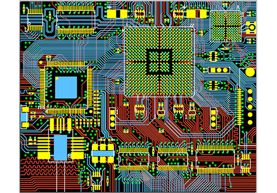
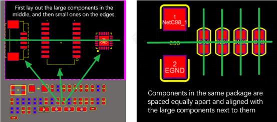
In PCB layout design, the layout of components is crucial. It determines the neatness and beauty of the circuit board and the length and number of printed circuits, which has a certain impact on the reliability of the entire machine. In addition to realizing the principle function, a good circuit board must also consider electrical characteristics such as EMI, EMC, ESD (electrostatic discharge), signal integrity, etc., as well as the mechanical structure and heat dissipation issues of high-power chips, ETC. This article puts forward some suggestions for general PCB layout for your reference. General PCB layout specification requirements Read the design documents to meet the layout requirements of special […]