What are Vias in Pad? Advantages, Limitations, Applications, and Comparison with Conventional Vias
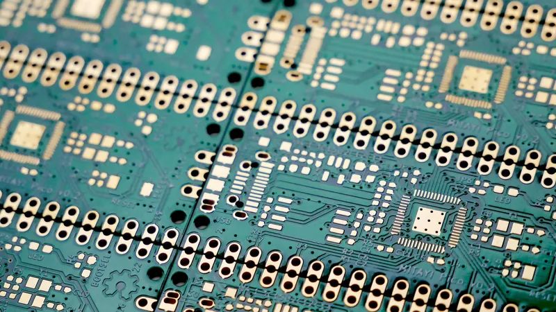
Vias go through two or more layers of PCBs to form an electrical connection. Making them right under the component’s pad saves space, reduces track inductance and simplifies design. Vertical interconnect access (or via) are small electrical connections that enable the transfer of electrical signals between different layers of a Printed Circuit Board (PCB). If we consider the tracks to be present in the x and y axes of the board, vias exist in the z-axis. Structurally, they are just like tiny coated vertical pipes plated with a layer of conductive material (such as copper/gold) and placed in a drill hole. They are also filled with different substances to ensure […]