High-speed ADC PCB layout and routing skills sharing
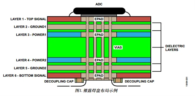
In designing a high-speed analog signal chain, there are many options to consider for printed circuit board (PCB) layout, some more important than others and some dependent on the application. The final answer varies, but in all cases, design engineers should try to eliminate deviations from best practices without obsessing over every detail of layout and routing. Exposed pad Exposed pad (EPAD) is sometimes overlooked, but it is very important to get the most out of the signal chain and to adequately dissipate heat from the device. The exposed pad, which Analog Devices calls pin 0, is the pad underneath most devices today. It is an important connection through […]