
Ball Grid Array (BGA) technology serves as the backbone for modern high-density electronics. Engineers rely on BGA soldering to connect advanced microprocessors and chipsets where traditional leaded packages fail. However, hidden solder joints beneath the component body introduce significant assembly complexity. Consequently, manufacturing teams must adopt precise methodologies to ensure interconnect reliability. This guide details the technical requirements for successful Ball Grid Array integration, from land pattern design to advanced rework protocols.
Understanding BGA Packaging Technology
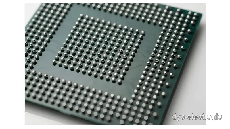
A BGA package features an array of solder balls directly contacting the PCB surface. This architecture enables several critical performance characteristics that define modern electronic design.
- High-Density Interconnections: Manufacturers can package integrated circuits containing over one thousand pads within a single BGA footprint.
- Compact Design: The grid array format maximizes board space utilization, making it ideal for space-constrained mobile and IoT devices.
- Improved Electrical Performance: Shorter signal paths reduce parasitic inductance, thereby enhancing high-speed signal integrity.
Despite these benefits, the concealed nature of the interconnections demands specialized BGA soldering expertise. Standard visual inspection methods cannot verify joint quality, necessitating advanced process controls throughout the assembly lifecycle.
Key Advantages Over Leaded Packages
Ball Grid Array packaging offers distinct improvements compared to conventional Quad Flat Package (QFP) or Dual In-Line Package (DIP) alternatives. These advantages drive adoption across automotive, medical, and consumer electronics sectors.
First, compactness remains a primary driver. BGAs occupy less board area while reducing overall device weight and height. Second, mechanical resilience improves significantly because solder balls resist physical damage better than fragile gull-wing leads. Third, manufacturing efficiency increases through direct surface mount compatibility, enabling faster automated placement. Finally, thermal performance optimizes heat distribution away from the die, reducing hotspots and extending component lifespan.
Nevertheless, engineers must address hidden joint challenges through rigorous Ball Grid Array assembly protocols. Ignoring these requirements risks catastrophic functional failures despite the inherent package advantages.
Critical BGA Soldering Challenges
Miniaturization and performance gains come with specific manufacturing hurdles. Identifying these challenges early prevents costly respins and yield loss during mass production.
Inspection complexity tops the list. Since joints remain invisible after reflow, technicians require X-ray imaging or acoustic microscopy rather than optical tools. Additionally, reworking defective units involves non-contact heating systems like infrared or hot air stations, which carry higher risk than standard iron-based repair. Thermal sensitivity also poses threats; improper profiles cause voiding, head-in-pillow defects, or pad cratering. Furthermore, positional accuracy during placement is paramount due to fine pitch dimensions typically ranging from 0.4mm to 0.8mm.
Addressing these issues requires sophisticated equipment alongside expert process engineering. Therefore, partnering with an experienced PCB assembly service ensures access to necessary metrology and rework infrastructure.
Essential BGA Soldering Process Steps
Achieving reliable interconnections demands mastery of five sequential stages. Each phase directly influences final joint metallurgy and long-term reliability.
PCB Land Pattern Design
Pad geometry must match the specific ball pitch of the component. IPC standards recommend pads slightly larger than the nominal ball diameter to accommodate registration tolerances. Non-solder mask defined (NSMD) pads generally provide better self-alignment during reflow than solder mask defined (SMD) variants for fine-pitch devices.
Solder Paste Deposition
Laser-cut or electroformed stencils are mandatory for consistent volume transfer. Engineers must calculate aperture ratios carefully to prevent bridging or insufficient wetting. Specifically, paste volume should correlate precisely with ball size to avoid void formation during the liquidus phase.
Precision Component Placement
High-speed pick-and-place machines utilize vision systems for centering verification. Accurate alignment enables the self-centering effect driven by molten solder surface tension. Misalignment beyond 25% of pad width typically results in open circuits or shorts after reflow.
Reflow Profile Optimization
SMT reflow profile development for BGAs requires tighter tolerances than through-hole or large passive components. Preheat ramps must stay below 3°C/s to prevent flux spattering. Soak zones activate flux chemistry uniformly across the thermal mass. Peak temperatures typically reach 245°C–250°C for SAC305 alloys, with time-above-liquidus maintained between 45–90 seconds. Controlled cooling rates below 4°C/s minimize grain coarsening and residual stress.
Advanced Joint Inspection
Post-reflow verification combines Automated X-Ray Inspection (AXI) with selective acoustic microscopy. These technologies detect internal voids, non-wetted pads, and misaligned spheres that escape optical detection. Referencing IPC-A-610 Class 3 acceptance criteria establishes objective quality benchmarks for void percentage and standoff height.
Professional BGA Rework Strategies
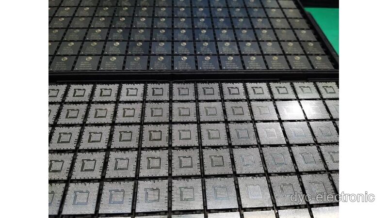
Even with optimized processes, defects occasionally occur. Successful BGA rework process execution restores functionality without damaging adjacent components or laminate layers.
Preparation begins with root cause analysis of the initial failure. Technicians then apply uniform heat via infrared or focused hot air to remove the faulty device safely. Site redressing follows immediately; this involves wicking residual solder, cleaning flux residues, and applying fresh no-clean or water-soluble flux. Reballing may be required if the original component is reusable, utilizing precision stencils to deposit new spheres. Finally, replacement and reflow must replicate the validated production thermal profile exactly.
Process control documentation validates each rework step. Without traceable parameters, reliability data becomes meaningless for safety-critical applications.
Ensuring Long-Term Reliability
BGA soldering represents a complex but manageable procedure when supported by appropriate technology. Invisible interconnections deliver exceptional electrical performance provided engineers respect their unique constraints. While challenges persist throughout product lifecycles, methodological rigor combined with advanced metrology ensures sustained operational integrity.
Frequently Asked Questions About BGA Soldering
What makes BGA soldering different from QFP assembly?
Unlike QFPs with visible peripheral leads, BGA soldering involves hidden connections underneath the package body. This concealment prevents optical inspection and requires X-ray verification. Additionally, self-alignment during reflow is more pronounced due to symmetric ball distribution, demanding precise thermal uniformity across the entire component footprint.
How do you inspect hidden BGA solder joints?
Technicians employ Automated X-Ray Inspection (AXI) as the primary method for Ball Grid Array assembly verification. AXI reveals internal voids, bridging, and non-wetting defects. Acoustic microscopy supplements X-ray by detecting delamination or cracks within the package substrate. Both methods are essential since visual examination only confirms external alignment markers.
What causes head-in-pillow defects in BGA reflow?
Head-in-pillow occurs when the solder ball and paste deposit fail to merge during liquidus phase. Common causes include insufficient paste volume, excessive warpage, or oxidized sphere surfaces. Optimizing stencil aperture design and verifying component coplanarity before placement typically resolves this SMT reflow profile issue. Moisture absorption leading to outgassing during reflow also contributes significantly.
Can BGA components be reworked multiple times?
Most PCB laminates withstand 2-3 rework cycles maximum before pad adhesion degrades or barrel plating cracks. Each thermal excursion stresses the FR-4 material and copper interfaces. Engineers should document cumulative thermal exposure per site. Using low-melt solder alloys for subsequent repairs can reduce peak temperatures and extend board service life.
Why is moisture sensitivity critical for BGA packages?
BGA substrates absorb ambient humidity rapidly due to organic materials. During reflow, trapped moisture expands violently, causing internal cracking known as “popcorning.” IPC/JEDEC J-STD-033 defines handling procedures including dry storage and pre-bake schedules. Adhering to these protocols prevents catastrophic BGA rework process failures and ensures long-term field reliability.
 Español
  English
  Русский
  Français
  Deutsch
  日本語
日本語  한국어
한국어  Português
  العربية
  Türkçe
  Italiano
  Polski
  Dansk
Dansk